Thank you to all those who attended our annual open day in 2025!
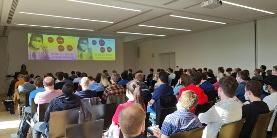
This year's event premiered a new blitz talk format, sparking enthusiastic conversations during lunch and coffee breaks. Dr. Maik Stappers gave the annual MNF update and students presented their research during a poster session, competing for the "Best Poster Award." Full details and pictures of the event are on our MNF Day page.
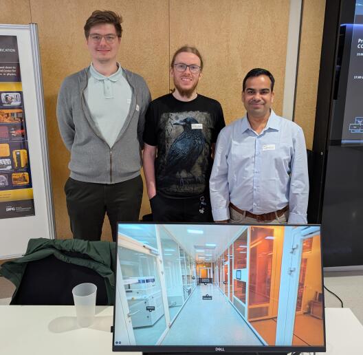
Premiering the 360° MNF Cleanroom Tour at the Quantum 100 Event
We presented our new 360° cleanroom tour at the national Quantum 100 event in Münster, where representatives from education, science, and industry showcased exciting technological achievements from 100 years of research and development in the field of quantum technology.
Ein Team um den Physiker Prof. Dr. Carsten Schuck und den Studenten Lukas Schulte sowie die Doktoranden Tim Buskasper und David Lemli hat den weltweit kleinsten QR-Code hergestellt. Mit einer Größe von 5,38 Quadratmikrometern ist er rund 20 Mal kleiner als der bisherige Weltrekord einer Forschungsgruppe aus Singapur und etwa siebenmal kleiner als eine menschliche rote Blutzelle. Die Arbeitsgruppe produzierte das Fabrikat mithilfe eines Elektronenstrahllithographie-Gerätes in den Reinräumen der „Münster Nanofabrication Facility“ (MNF). Hier arbeiten Forscherinnen und Forscher verschiedener Fachrichtungen sowie Masterstudierende im Praktikum „Grundlagen der Nanofabrikation“. „Die technische Ausstattung in der MNF ist hochmodern und kommt neben unseren Forschungsaktivitäten in der Quantentechnologie unseren Studierenden in innovativen Lehrformaten zugute, die in Praktika nanoskalige QR-Codes herstellen – wenn auch etwas größer als bei unserem Rekordversuch“, unterstreicht Carsten Schuck.
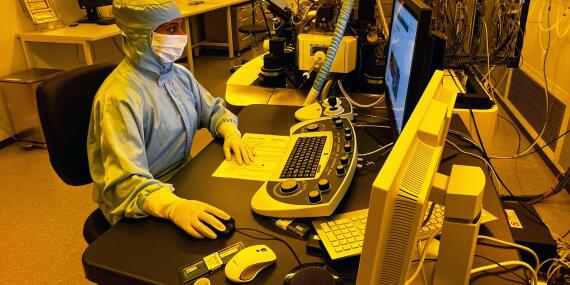
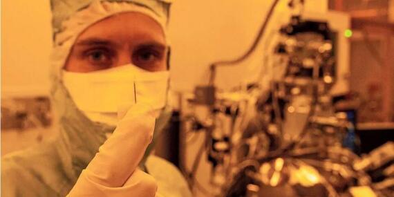
In den Reinräumen der Münster Nanofabrication Facility haben Studierende und Forschende die Möglichkeit, mikroskopisch kleine Strukturen herzustellen, die mit bloßem Auge kaum zu erkennen sind. Sauberkeit ist das höchste Gebot: Ein Haar oder Staubpartikel könnte das Experiment zerstören. Die Teilnehmerinnen und Teilnehmer des Praktikums „Grundlagen der Nanofabrikation“ müssen sich daher an genaue Vorschriften halten.
New project to protect critical infrastructure against cyberattacks
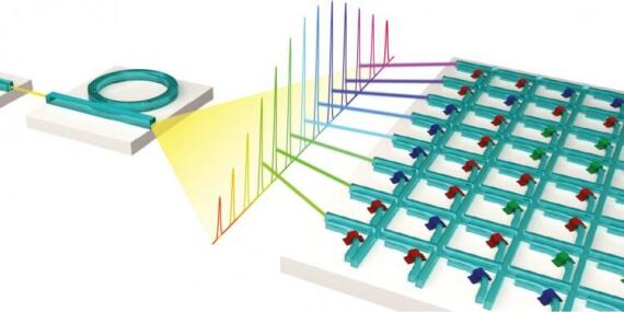
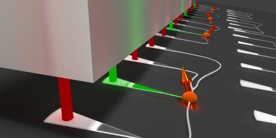
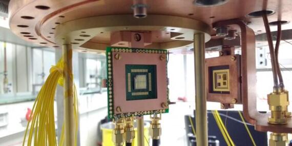
Carsten Schuck’s research group is designing, building and testing a receiver unit for a quantum key generation process and the operation of secure communication in a gas pipeline system produced by PSI Software SE. “Any attempt at eavesdropping would be noticed immediately, rendering the key generation system independent of the measuring devices,” explains Carsten Schuck. His team is building this system at the Münster Nanofabrication Facility (MNF) using a special technology designed in-house. It uses superconducting single-photon detectors which are embedded in advanced photonic integrated circuits. The circuits are embedded in chips that are cooled to around two Kelvin in order to make the best possible use of their superconducting properties.
Physicist Dr. Shabnam Taheriniya has been awarded the Infineon Doctoral Prize 2024, endowed with 3000 euros, for her excellent doctoral thesis at the University of Münster. For her dissertation in Professor Gerhard Wilde's working group at the Institute of Materials Physics, she investigated the inner interfaces in a new class of materials known as high-entropy alloys, analyzing the mixture of high-entropy alloys with different crystal structures forced by intensive plastic deformation. Dr. Taheriniya also investigated the behavior of the materials under irradiation with fast, heavy ions as well as their microstructure and the inner interfaces and their magnetic behavior using transmission electron microscopy methods in the Münster Nanofabrication Facility (MNF).
The Department of Physics at the University of Münster awards the Infineon Doctoral Prize annually together with Infineon AG.
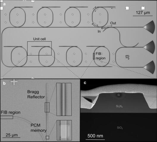
Congratulations to Anna Ovvyan for winning third place for her image "Capillary-photonic integrated circuit based on integration of semiconducting CNTs." By making use of our EBPG5150, she integrated one-dimensional electroluminescent semiconducting carbon nanotubes into hybrid two-dimensional/three-dimensional photonic circuits. Using 2D nanographene as a low-loss material to electrically contact sCNT emitters directly within a photonic crystal cavity, she achieved efficient coupling and enhancement of electroluminescent without compromising the optical quality of the cavity. This versatile approach paves the way for controllable integrated photonic circuits.
And congratulations also to Akhil Varri, who received the Honorable Mention and Art Award for his image "Wavelength addressable photonic memory."
Both the cleanroom and the high-tech equipment park in the Münster Nanofabrication Facility (MNF) are used by people from a variety of disciplines such as Physics, Chemistry, Geosciences and Biology. As a central university institute within SoN, the MNF can be used by researchers from both inside and outside the University.
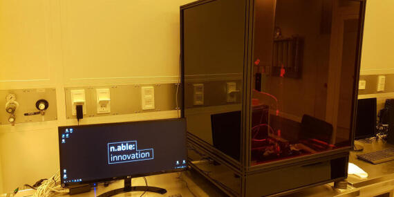
Join us at our upcoming Molecular Printer Workshop, on July 27th from 9 am-3 pm in the SoN. During the workshop, n.able GmbH will give a general introduction to the machine, discuss potential applications and conduct in-person, hands-on training. We encourage you to bring along your own chip substrates and molecules for test printing.
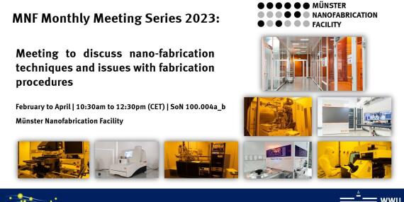
We are pleased to offer you additional support on improving your fabrication methods at our monthly fabrication meeting. Please join us to ask questions and discuss any issues with fabricating your samples.
When: first Friday of the month, February to April, 10:30am-12:30pm Where: Center for Soft Nanoscience (SoN) seminar room
Melissa Pernice won second place in the international Moodle photography competition for her picture of our engineer, Riya Gupta, using Learnweb while sitting at the Zeiss ORION NanoFab.
MNF scientists are trained on working in the cleanrooms through tutorials created using the open-source learning platform Moodle (called "Learnweb" at the University of Münster).
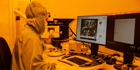
„Wir kommen gleich an einen der saubersten Orte Münsters", sagt der Nano-Strukturtechniker Dr. Johannes Kern. Spezielle Technik saugt jedes Staubkorn aus der Luft. Denn ein Staubkorn kann hier beim entsprechenden Versuch wie ein Komet wirken.
Johannes Feldmann was awarded the Infineon Doctoral Prize 2021, worth 2,500 euros, for his outstanding doctoral thesis. The physicist from Professor Wolfram Pernice's research group worked with Professor Harish Bhaskaran's group at the University of Oxford to develop neuromorphic photonic processors. Using infrastructure in the Münster Nanofabrication Facility, Dr. Feldmann developed photonic processors that allow a particularly high number of arithmetic operations to be performed per chip area. To do this, he used so-called phase change materials, creating artificial neural networks that only work with optical methods. These networks can learn independently and recognize patterns.
The Department of Physics at the University of Münster awards the Infineon Doctoral Prize annually together with Infineon AG.
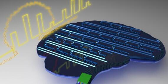
The PHOENICS project (the acronym stands for “Photonic enabled petascale in-memory computing with femtojoule energy consumption”) aims to give a boost to the development of new computing resources. The researchers involved plan to create so-called photonic neuromorphic processors with unprecedented computing power and energy efficiency. In this case, “neuromorphic” means that the processors take inspiration from the human brain and that the information is processed and stored in one and the same place. In the case of traditional computers, the computing and data storage units are separate from each other. “Photonic” means that data are transported by means of light instead of electrons (as in traditional computers).
In the project, the PHOENICS consortium plans to use new types of materials to create the photonic neuromorphic processors. Another aim is to develop new methods of significantly increasing computing power.
“Exploiting light for signal transference enables the processor to perform parallel data processing through wavelength multiplexing, which leads to a higher computing density and many matrix multiplications being carried out in just one timestep. In contrast to traditional electronics, which usually work in the low GHz range, optical modulation speeds can be achieved with speeds up to the 50 to 100 GHz range.” This means that the process permits data rates and computing densities, i.e. operations per area of processor, never previously attained.
Researchers at the University of Münster have now succeeded for the first time in fully integrating nanodiamonds into nanophotonic circuits and at the same time addressing several of these nanodiamonds optically. In the process, green laser light is directed onto colour centres in the nanodiamonds, and the individual red photons generated there are emitted into a network of nano-scale optical components. As a result, the researchers can now control these quantum systems in a fully integrated state. The results have been published in the journal “Nano Letters”.
Mostafa Amirpour, our second cleanroom engineer, recently joined the MNF. Mostafa has an electrical engineering background. Prior to coming to Münster he was a cleanroom fabrication engineer and electronic sensor test engineer at the University of Urmia, Iran. He has a hands-on experience in various silicon micromachining technique including PVD, wet etching, anodic and fusion bonding and photolithography.
For those who want to learn more about gowning at the MNF, we put together a video detailing the procedure step-by-step. Click on the link below to watch it now, or log in to our Learnweb course to see the video and complete some practice lessons.
“I conduct secondary ion mass spectroscopy (SIMS) analysis using the Tof-SIMS, a device for 3D chemical imaging down to 100 nanometer resolution. Essentially, I take materials and discover not only their chemical composition, but the way those chemical species are distributed in three dimensions. My personal research seeks to improve ToF-SIMS sensitivity, spacial resolution and data interpretation. I also apply the ToF-SIMS technique in collaboration with other research projects at the Center for Soft Nanoscience (SoN).
Welcome to our newest member of staff, Riya Gupta! Riya is joining us as a Nanoanalytics Engineer. She will be working in the cleanrooms maintaining and offering training and support for instruments including the SEM, SNOM, AFM, and FIB. She worked previously as a research fellow at the International Iberian Nanotechnology Laboratory in Portugal, where she developed portable electrochemical sensors for monitoring water contaminants.
Riya is excited to share her expertise and enthusiasm for Nanoanalytics with everyone and looks forward to becoming an expert on our instruments.
My research is in integrated optics. We do nanofabrication. I truly enjoy working in the cleanroom doing the whole fabrication process from start to finish, making a chip that you can finally measure...The cleanroom (Münster Nanofabrication Facility): having all these machines in one place is not common. Here we can do nanofabrication of very complex chips from the very first to the last steps. There are not many other locations in Europe that are comparable.
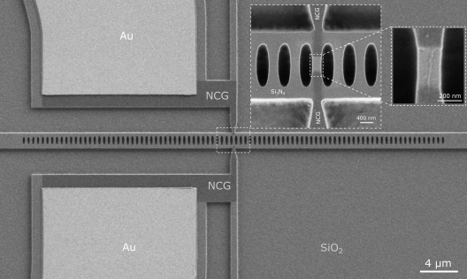
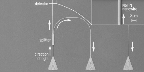
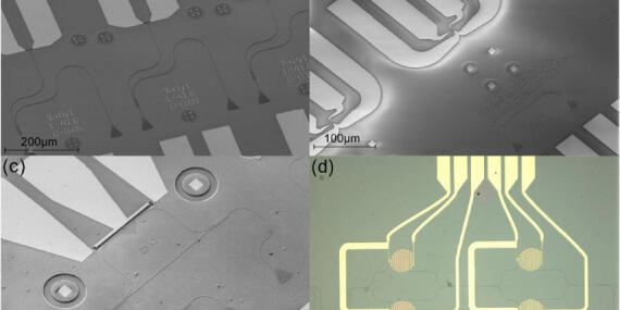
Martin Wolff was selected for second place by Raith for his research using the Raith system in the Münster Nanofabrication Facility (MNF). Wolff, a student in Research Group Schuck, created a waveguide-integrated superconducting nanowire single-photon detector device.
His device is made of three elements: 1) gold contact pads used for electrical connections, 2) a superconducting nanowire placed between the gold pads, which is sensitive to single photons, and 3) a dielectric waveguide coupling structures for coupling light on the chip to the detector. The detection speed of his detectors easily reaches GHz counting rates and offers high efficiencies of over 90%, dark count rates in the mHz regime, and timing uncertainties (jitter) of a few picoseconds over a wide optical window, especially in the telecommunication band.
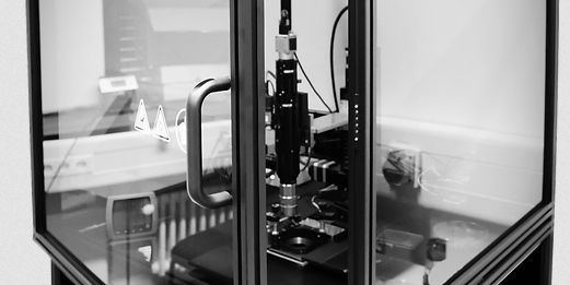
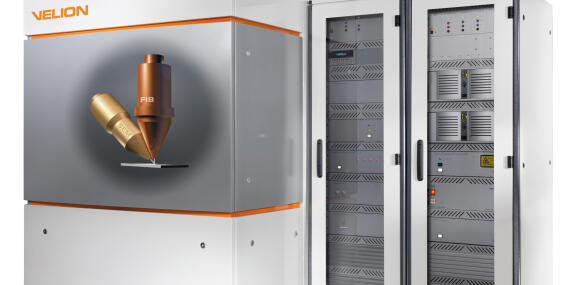
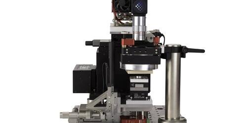
"From the outside, the instrument, located on the ground floor of the Center for Soft Nanoscience (SoN) at Münster University, is just a grey cupboard the size of two wardrobes – but inside there is a lot going on. The centrepiece of the equipment is a focused ion beam and a scanning electron microscope. The ion beam enables structures to be “written” in thin layers – for example, to produce circuits on chips. What is special about the instrument is a special ion source with charged gold and silicon atoms. Compared with equipment using gallium ions, which are the ones normally used, this instrument enables the researchers to structure the material more precisely, generate larger-sized structures and thus fill up for example entire wafers, as used in the semiconductor industry. The process also means that many small points can be arranged side by side and joined up with one another. The microscope simultaneously scans the surface of the materials and creates high-resolution images of the molecular structures in order to monitor the process. This type of instrument is the only one of its kind so far in Germany..."
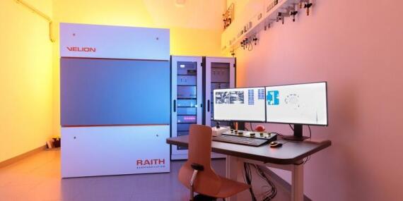
With the new Raith VELION possible EBL instrumentation and FIBL applications in plasmonics and nanophotonics include:
plasmonic arrays and zero mode waveguides for sensing biological molecules
solar absorber arrays
color center creation by maskless ion implantation
large area photonic structures in diamond
and metallic metasurfaces.
Additionally it's possible to apply Gallium or non-Gallium species, such as Silicon, Gold, Germanium, Lithium, Bismuth and clusters, and to use workflows to generate lamellas for transmission electron microscopy (TEM) analyses.
On March 5th, 2020, MNF scientists attended a presentation by Dr. Torsten Richter Product Manager, Raith GmbH, covering the above topics and more
"Researchers working in the MNF demonstrate for the first time energy quantization in nanowires made of high-temperature superconductors- where the temperature is brought to the level below which quantum mechanical effects predominate. The results are published in the journal Nature Communications."
The MNF has received a five-year grant from the DFG to establish its machine-park, cleanrooms and laboratories as a core university facility. With plans to expand its interdisciplinary user base, establish a support team, and create interactive online training, the MNF is on track as a cutting-edge facility for nanofabrication and nanoanalytics in Münsterland.
GDSHelpers is a Python-based, easy-to-learn, open-source software package, which allows users to quickly generate arbitrary photonic and other devices. Users can automate pattern generation for nano-structuring and export patterns in GDSII- and OASIS-format (for describing 2D-masks). Currently, the focus is mainly on photonic and superconducting circuitry.
The Python library GDSHelpers holds a growing list of parts, which can be composed into larger circuits.
"Researchers at the University of Münster have now developed an interface that couples light sources for single photons with nanophotonic networks. This interface consists of so-called photonic crystals, i.e. nanostructured dielectric materials that can enhance a certain wavelength range when light passes through. Such photonic crystals are used in many areas of research, but they had not previously been optimized for this type of interface. The researchers took particular care to achieve this feat in a way that allows for replicating the photonic crystals straightforwardly by using established nanofabrication processes."
The TERA-Fab™ E series is the world’s first beam pen lithography (BPL) tool, which provides the user with a way to prototype functional electronic devices, perform highly-localized photochemistry relevant to biology and medicine, and make the types of architectures traditionally made with photolithography, but in a mask-free fashion and with a diffraction-unlimited, sub-250 nm resolutions. With the E series, the user can rapidly create nanopatterns of any design across square micrometer to tens of square millimeter areas using a wide range of photosensitive materials.
On the 6th of November 2019, MNF scientists had the opportunity to learn more about the TERA-Fab™ E series from Dr. Andrey Ivankin, the chief technology officer and co-founder at TERA-print.
An international team of researchers from the Universities of Münster (Germany), Oxford and Exeter (both UK) have now succeeded in developing a piece of hardware which could pave the way for creating computers which resemble the human brain. The scientists managed to produce a chip containing a network of artificial neurons that works with light and can imitate the behaviour of neurons and their synapses.
A giant cylindrical refrigerator, an electron-beam pattern generator, a cleanroom, etching equipment. Sometimes it takes a lot of big things to make something very small. The nanoscientists at the University of Münster headed by Prof. Wolfram Pernice and Prof. Carsten Schuck know this only too well: they use these and other devices to produce nanophotonic chips the size of a one-cent piece. These small chips, which also contain much smaller functional structures, can do a great deal – for example, contribute to the tap-proof transmission of data.
The new state-of-the art molecular printer installed in the Münster Nanofabricaton Facility (MNF) addresses the needs of users working in various fields of nanoscience ranging from biomedicine, material sciences to microelectronics. Allowing for flexible choice and combination of various functional modules, it can cover a wide range of applications and research projects, and has the following features:
Base printing module with a choice of different printing technologies (ranging from cantilever arrays and soft polymeric stamps to microcapillary pens)
High-Resolution module for increased patterning control down to the low nanoscale
Climate module for controlled humidity
Optical module for in-situ process control and analysis.
On the 4th and 5th of November 2019, MNF scientists participated in a workshop to learn more about this exciting new technology.
We are pleased to announce the new molecular surface patterning system installed in the Münster Nanofabrication Facility (MNF) at the Center for Soft Nanoscience (SoN). Thanks to its modular design, the printer addresses the needs of users working in various fields of nanoscience ranging from biomedicine, material sciences to microelectronics.
Das ist einzigartig. Da die Forscher in einem Gebäude arbeiten, werden sie sich häufiger treffen: geplant in den Kolloquien und Seminaren, aber auch zufällig bei der Kaffeemaschine. Sie werden sich also schneller und besser kennenlernen und daher eher auf neue gemeinsame Ideen kommen. Vor allem ist auch die Durchführung von komplexen interdisziplinären Experimenten deutlich einfacher, weil die Forscher in benachbarten Laboren sind und teils sogar dieselben Labore nutzen.
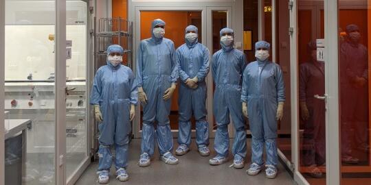
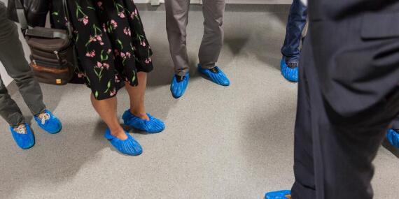
Der Reinraum ist für Besucher nicht zugänglich – zu groß ist die Gefahr, dass auch nur ein einziges Staubkorn die Arbeit verfälschen könnte. Alle Mitarbeiter dürfen den Raum nur mit Schutzkleidung betreten, um keine Verunreinigungen einzuschleppen. Im sogenannten Grauraum, der den Reinraum u-förmig umgibt und der bereits deutlich staubfreier ist als jedes Standardlabor, spürt man einen stetigen, kalten Luftzug. Er entsteht durch die aus dem Reinraum strömende Luft – dort drinnen herrscht permanent ein Überdruck, damit keine ungefilterte Luft hineinströmen kann.