
Contents
- Electron beam lithography - Raith EBPG5150
- Dual beam Si/Au Focus Ion Beam (FIB)/ SEM - Raith VELION
- Beam pen lithography- TERA-print
- Polymer pen lithography- n.able Molecular Printer
- Mask aligner - Karl Suss MA56
- Nano Imprint Lithography System - EVG620 NT
- Nanoscribe Quantum-X Align
- 3D Lithography - Nanoscribe Photonic Professional GT
- Helium/Neon Focused Ion Beam (FIB) – Zeiss ORION NanoFab
Lithography
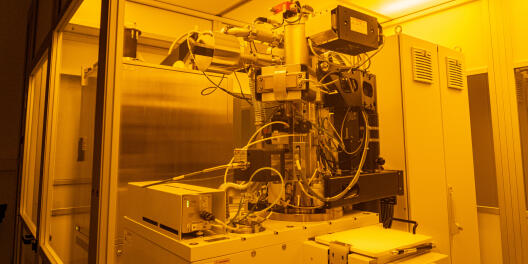
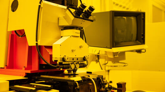
Electron beam lithography - Raith EBPG5150
- High current density Thermal Field Emission gun for operation at 20, 50 and 100 kV
- ISO 5 environmental chamber
- 155 mm x 155mm stage
- Mimimum feature size of less than 8 nm
- Rapid exposure with 50 or 100 MHz pattern generator
- Continuously variable large field size operation to 1 mm at all kVs
- GUI for ease of use operation for diverse "multi user environment"
Contact: Adrian Abazi
Back up contacts: Ivonne Bente, Dmitrii Raskhodchikov
Location: CeNTech II, E-beam zone
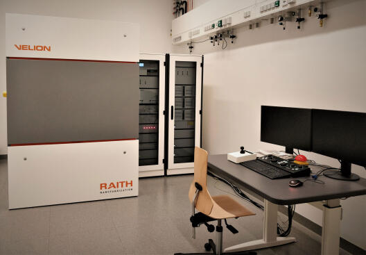
Dual beam Si/Au Focus Ion Beam (FIB)/ SEM - Raith VELION
- Silicon or Gold focus ion beam (main column)
- SEM for imaging
- Ion-assisted electron beam lithography
- Direct milling
- Tungsten GIS
- Continuous writing/ stitch-free lithography
- TEM lamella preparation with live SEM control
Contact: Akhil Vari, Tim Buskasper
Location: SoN, lab 100.045
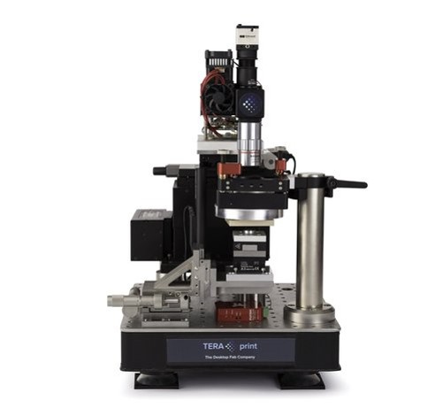
Beam pen lithography- TERA-print
- Massively parallel cantilever-free scanning probe lithography for large0area, low-cost and arbitrary surface patterning
- Rapid generation of micro and nano structures using the PPL head comprised of 20,000 independently addressable pens (NSOM tips)
- Feature size resolution of sub-200 nm
- Patterning area: 0.5 x 0.4 cm2
Contact: Maik Stappers
Location: SoN, nanochemistry zone
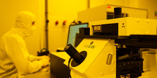
Polymer pen lithography- n.able Molecular Printer
- Base printing module with a choice of different printing technologies (ranging from cantilever arrays and soft polymeric stamps to microcapillary pens)
- High-Resolution module for increased patterning control down to the low nanoscale
- Climate module for controlled humidity
- Optical module for in-situ process control and analysis.
Contact: Riya Gupta
Location: SoN, nanochemistry zone
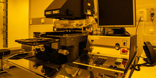
Mask aligner - Karl Suss MA56
-
Configured for 5" wafers
-
UV400 Exposure Optics (for 365 nm and 405 nm exposure)
-
Capable of Hard Contact, Soft Contact and Proximity Exposure Modes
Contact: Johannes Kern
Location: CeNTech I, preparation zone, 0.15
Nano Imprint Lithography System - EVG620 NT
- Semi-automated system
- Configured for 2" or 4" wafers
- UV400 exposure optics (for 350 nm - 450 nm exposure)
- Capable of hard contact, soft contact and proximity exposure modes
- UV-Nanoimprint lithography and microprinting to achieve sub 100 nm features
Contact: Maik Stappers
Location: SoN, photolithography zone
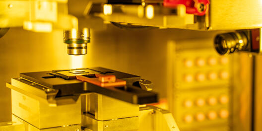
Nanoscribe Quantum-X Align
- Two-photon lithography of common positive-tone photoresists
- High speed 3D printing by galvo technology
- High resolution micro 3D printer
- voxeltuning for fabrication of 2.5D topography
- up to 50mm large structures
- down to 100nm small structure sizes
- maximum print area of 50x50mm²
Contact: Daniel Wendland
Location: CeNTech I, preparation zone, 0.15
3D Lithography - Nanoscribe Photonic Professional GT
- Writing area up to 100 × 100 mm² range
- Two-photon lithography of common positive-tone photoresists
- Two photon polymerization (2PP) of various UV-curable photoresists
- High speed 3D printing by galvo technology
- High resolution micro 3D printer
Contact: Daniel Wendland
Location: CeNTech I, preparation zone, 0.15
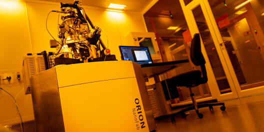
Helium/Neon Focused Ion Beam (FIB) – Zeiss ORION NanoFab
- Scanning helium ion microscope,
- 0.5 nm imaging resolution
- SE, secondary electron detector
- Focused Ion Beam milling using He and Ne ions;
- Nanostructures with sub-10nm dimensions
- Coming soon: Raith Elphy pattern generator
Contact: Riya Gupta
Location: SoN, FIB zone