AG Schuck
AG Schuck

Integrated Quantum Technology

In our research we aim at developing quantum technology for single-photons on silicon chips. We design, fabricate and test photonic devices using advanced nanotechnology that allows for straightforward replication of functional units. Our activities focus on three core constituents of chip-scale quantum optics:

  • Design of efficient interfaces between optical waveguides and single-photon sources.
  • Development of nanophotonic devices and quantum circuit components. 
  • Integration of superconducting nanowire single-photon detectors with nanophotonic waveguides.

Combining all three of these research directions leads to scalable quantum information processing with tremendous benefits over classical computation and communication systems.

  • Single-photon sources

    Integrated single-photon sources

    Single-photons are attractive information carriers because they are robust against decoherence effects and allow for high-speed manipulation and communication. We hence consider single-photon sources a key resource for quantum technology, in particular quantum information processing, as well as novel sensing applications, e.g. super-resolution imaging and biomarking. We are investigating several approaches to making single-photons available on silicon chips. One of our main objectives is to integrate quantum light sources directly with nano-photonic waveguides. This can be achieved either via strongly nonlinear optical processes or by coupling nano-scale single-photon sources via suitable interfaces to optical waveguides. Using advanced nano-fabrication techniques we aim at integrating and controlling a large number of such quantum emitters that supply single-photons to an optical network directly on a nano-photonic chip.

    In previous work we have succeeded in generating photon pairs in nano-photonic waveguides from a strong pump laser beam in the process of spontaneous parametric down-conversion (SPDC). This process requires a material system with strong second-order nonlinear coefficient. We therefore performed extensive preliminary work on the nonlinear optical properties of several waveguide material systems. In particular gallium nitride (GaN) and aluminum nitride (AlN) were identified as promising candidates because both feature strong second-order nonlinearities, as we demonstrated via the observation of efficient second harmonic generation (SHG). For generating photon pairs in SPDC we then adapted the phase-matching conditions inside an AlN-micro-ring resonator yielding photon pairs at MHz-rates. The non-classical nature of these down-converted photons was confirmed by measuring strong antibunching (g(2)(τ=0) < 0.09) of signal photons heralded by the detection of their partner (idler) photon.

    In future work we will focus on heterogeneous integration of solid-state quantum systems, e.g. fluorescent nano-crystals and colloidal quantum dots, with nano-photonic waveguide structures. Nanotechnology offers many possibilities of building efficient interfaces between quantum emitters and optical waveguides as the emission and absorption properties of a quantum system can be manipulated with customized photonic and plasmonic structures, e.g. photonic crystal cavities and nano-antennae, respectively. We study the emitter-waveguide coupling-conditions to enable controlled single-photon production as well as investigating the photo-physical properties of integrated luminescent sources.


    Information on our previous work is found here:


  • Nanophotonic Circuits

    Nanophotonic devices and quantum circuit components

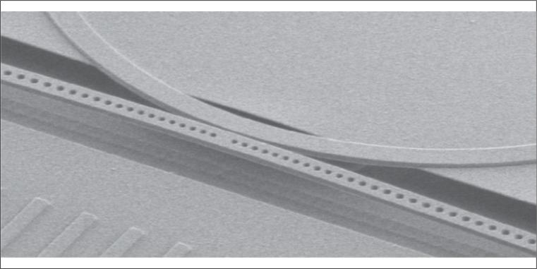
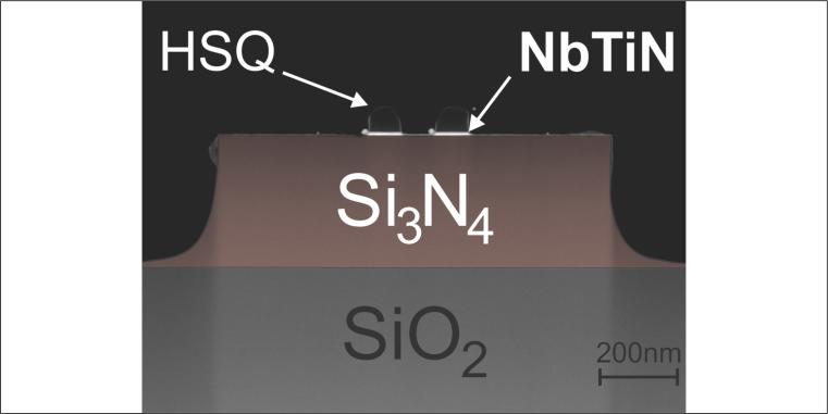
    Nano-photonic devices can be patterned out of dielectric thin-films by employing electron beam lithography and a variety of associated etching techniques. A wealth of photonic integrated circuit components has been developed within the silicon photonics community for classical telecommunication tasks. The high refractive index contrast between silicon, as the optical medium, and an insulating substrate, e.g. silicon dioxide, allows for tightly confining optical modes in waveguides of submicron cross section. On the one hand, this allows for very compact and densely packed nano-photonic circuits and on the other hand, it is possible to engineer the group velocity dispersion by fine-tuning the waveguide geometry. Using a computer aided design approach and advanced nano-fabrication techniques we are further able to integrate such nano-photonic devices with electrical circuits and mechanical structures. The inherent mechanical stability of monolithic silicon chips significantly benefits the implementation of nested optical interferometers yielding highly stable phase contrast. Combining optical, electrical and mechanical capabilities on a chip gives rise to interesting novel functionality as we have shown in previous work on high-frequency optomechanical resonators, high-quality factor photonic crystal cavities, and even piezo-electrically actuated nano-cavities.

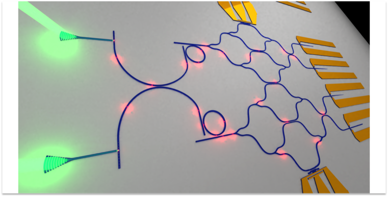
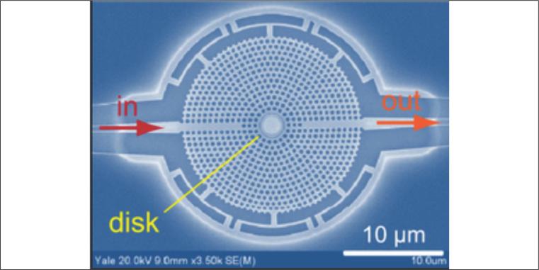
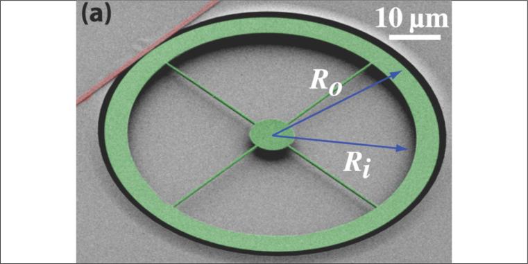
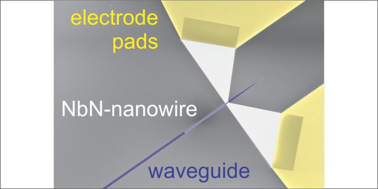
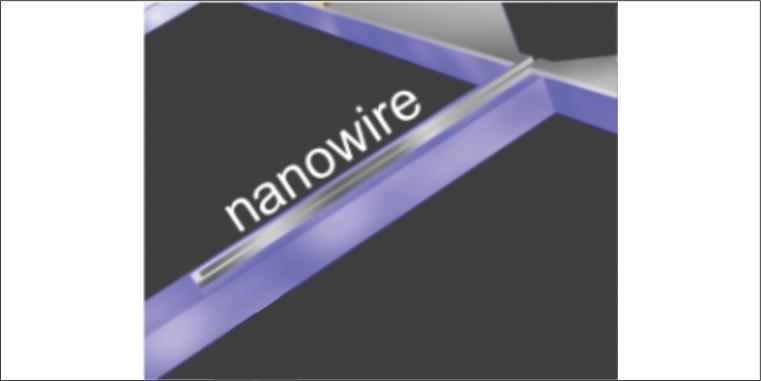
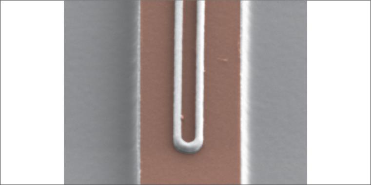
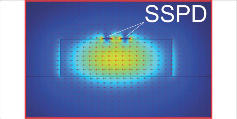
    Many established photonic integrated circuit components can be adapted to fulfill the demands of quantum technology with single photons. We have demonstrated this for some crucial nano-photonic devices, for example directional couplers, optical phase shifters, bandwidth filters, ring-resonators and grating couplers. Our implementation of a directional coupler with well-controlled optical mode splitting ratio– the equivalent of a bulk optic beam splitter – was particularly important for demonstrating quantum interference in a silicon nitride (SiN) waveguide circuit. Embedding superconducting nanowire single-photon detectors into this circuit allowed us to measure two-photon (Hong-Ou-Mandel) interference with a visibility of 97%, which demonstrates the suitability of an integrated optics approach for quantum information processing. In future work we will elaborate on these studies by fabricating more complex circuits with an increasing number of nano-photonic components thus realizing quantum gate operations, which can then be concatenate to assemble quantum algorithms.   

    Information on our previous work is found here:


  • Superconducting Single-Photon Detectors

    Waveguide integrated superconducting nanowire single-photon detectors

    The principal method in quantum optics to obtain information about a quantum system is photo-detection. In previous work we developed a novel type of superconducting nanowire single-photon detector (SNSPD), which seamlessly integrates with nano-photonic waveguides. We fabricate wires of a few tens of nanometer width from superconducting thin-films in electron beam lithography and reactive ion etching. These nanowires are then positioned on top of sub-micrometer sized optical waveguides such that photons are efficiently absorbed as their electrical field is attracted to the superconducting metal. In this travelling wave geometry typically more than 95% of all photons inside a waveguide are absorbed along their direction of propagation over a length of a few ten micrometers. We have demonstrated such SNSPDs in a variety of material systems, combining niobium based superconductors (NbN & NbTiN) with several different substrates for operating both at visible wavelength (in wide-transparency SiN-waveguides) and near-infrared wavelengths (in the telecom C-band using Si-waveguides). A closed-cycle cryostat cools our devices below the critical temperature of the superconducting material and we current-bias the nanowire-detectors just below their critical current. Under such conditions even the absorption of a single-photon will drive the corresponding section of the nanowire into a normal-resistive state, hence causing a short voltage pulse that signals the photo-detection event. The detection mechanism relies on extremely fast carrier dynamics and is highly efficient over the entire wavelength range from the UV all the way to the near-IR. This enables us to detect photons inside a waveguide with up to 90% efficiency at several hundred MHz rates and a few ten picosecond timing uncertainty. Minimal detector footprint and appropriate choice of the superconducting material also allows for attractive low-noise operation of SNSPDs, featuring sub-Hz dark count rates.    

    In future work we plan on exploiting these attractive detector characteristics for integrated quantum technology applications. One of our goals is the integration of SNSPDs with quantum emitters on the same chip, directly linked via low-loss optical waveguides. Nano-photonic circuitry in-between emitter and detector will allow for additional functionality, e.g. to investigate statistical and spectral properties of waveguide-coupled quantum emitters. The low-loss waveguide interfaces will thus enable us to take full advantage of our detectors' high efficiency, low noise and high timing resolution over a large wavelength range. Combining multiplexed single-photon sources with ultrafast detection on the same chip then enables conditional operations on photons buffered in a photonic integrated circuit, therewith dramatically improving our ability to implement scalable quantum technology.

    Information on our previous work is found here: