Research overview
© AG Schlenhoff

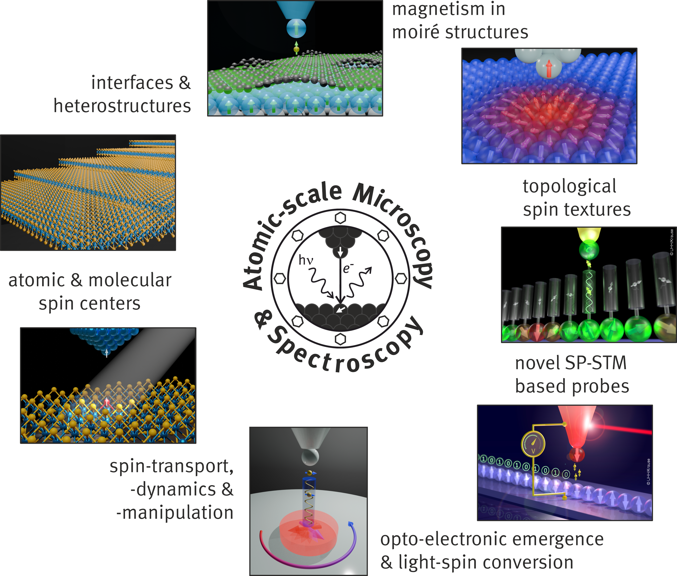
Our research group Atomic‑scale Microscopy & Spectroscopy, founded at the University of Münster at the end of 2022, focuses on the atomic‑scale investigation of correlations among structural, electronic, magnetic, and optical properties of low‑dimensional (magnetic) solid‑state systems. In addition, we aim to advance the methodological capabilities required for these investigations.

As illustrated above, our scientific interest spans the local characterization of atomic and molecular spin centers, the spatially resolved study of non‑collinear and topological spin textures in thin films and magnetic moiré structures, and the associated interfacial effects in two‑dimensional hetero‑ and hybrid structures. A further research focus is the atomic‑scale examination of spin transport, spin dynamics, and spin manipulation, together with the related charge‑spin conversion efficiency.

We have strong expertise in, and actively develop, our own innovative in‑house techniques based on spin‑polarized scanning tunneling microscopy (SP‑STM) and spin‑polarized scanning tunneling spectroscopy (SP‑STS), which are employed to investigate all of the aforementioned phenomena. The current portfolio is being expanded to include light‑assisted (SP‑)STM/STS methods, enabling the exploration of optically induced opto-electronic and magneto‑optical phenomena at the atomic scale by photo‑excitation of the (magnetic) tunneling junction.
Instrumentation

  • © AG Schlenhoff

    LT-STM/AFM with optical access

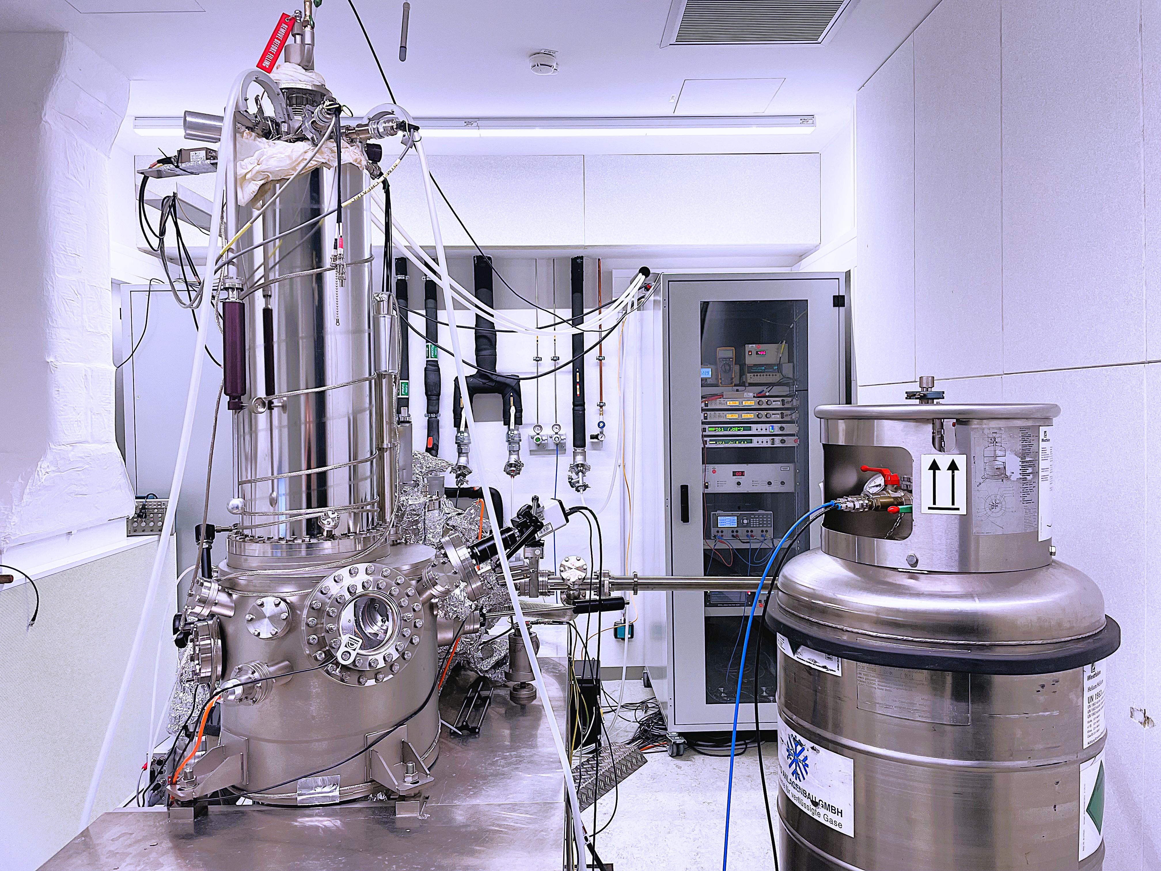
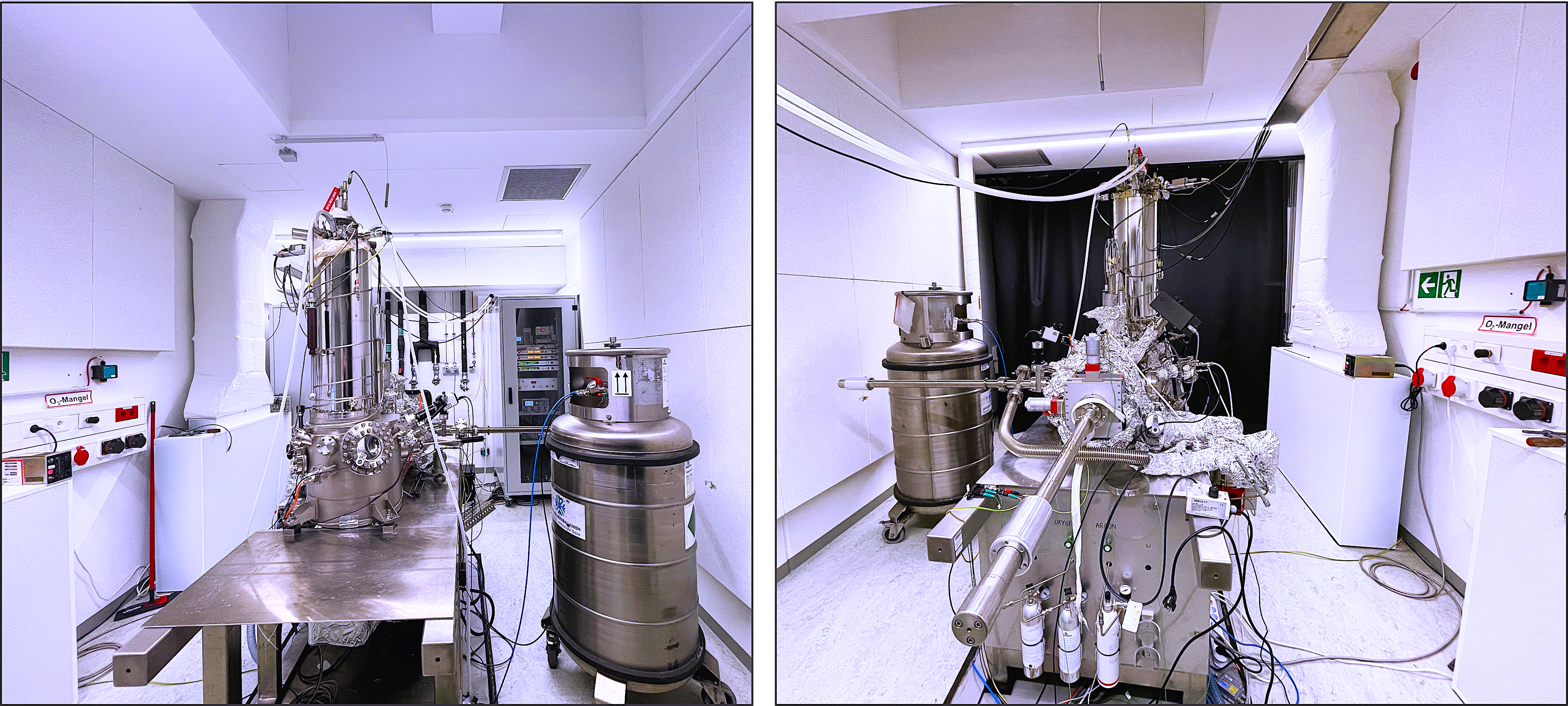
    Our laboratory is equipped with a combined Low-Temperature Scanning Tunneling Microscope/Atomic Force Microscope (LT-STM/AFM) operating at liquid Helium (<5K) and liquid Nitrogen (<78K) temperatures and under ultra-high vacuum (UHV) conditions. The guidance of light into and out of the tip-sample junction is realized via two dedicated optical accesses to the microscope in combination with in-situ lenses attached close to the probe tip-sample junction. An additional optical access to the junction allows single-atom deposition onto the cold sample within the microscope. We have standard in-situ tip and sample preparation techniques that we continuously expand to our needs. We are equipped with an Acton Pro Spectrometer with a cooled CCD camera for analyzing the light emission from the junction and with different light sources for light excitation of the junction.

    As a growing group we are developing novel instrumental setups tailored for our research objectives.

  • © AG Schlenhoff

    Tunable cw- and fs-light sources

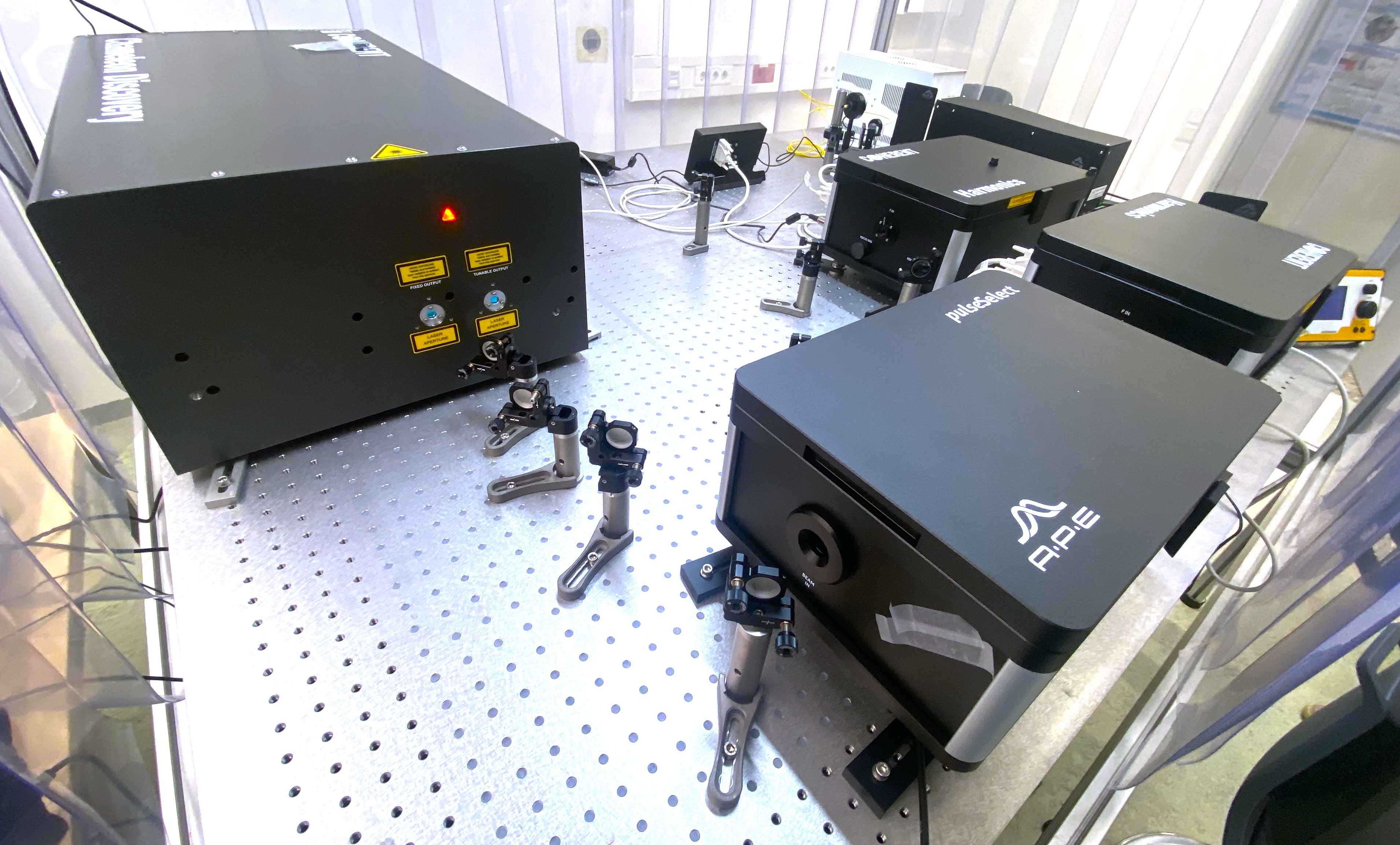
    Pulsed light source - Our femtosecond (fs) system is a widely tunable, hands‑free laser from Coherent that is equipped with second‑ and third‑harmonic generators. Together they provide continuous wavelength coverage from 227 nm to 1320 nm while preserving a 100 fs pulse duration and an 80 MHz repetition rate.
    A set of flip mirrors on the optical table lets us route the beam either straight to the experiment next‑door or into one of the two harmonic generators with a single click. In addition, a pulse‑selector can be inluded to lower the effective repetition rate of the pulsed source when needed.

    Continuous-wave light source - The tunable high‑brightness continuous-wave (cw) source is built by coupling a laser‑pumped plasma light source to a monochromator. This combination delivers an effective wavelength range from 350 nm to 1200 nm.
    Unlike conventional discharge lamps, the laser‑pumped plasma behaves almost like a point source; the size of the emitting plasma is defined by the focus of the pump laser. Consequently the output is easy to collimate and to focus onto the experimental sample.

  • © AG Schlenhoff

    Lab Infrastructure

    Our renovated and modernized basement facilities provide an optimal environment for (spin-polarized) STM/STS experiments with or without light stimuli. The central optical laboratory is located between two STM labs, enabling laser beams, broadband light and other optical probes to be delivered to either facility.

    The rooms are equipped with low-noise, high-precision air-conditioning, sound insulated doors, suspended ceilings and wall panels that absorb acoustic energy, dramatically reducing background vibrations and airborne noise. In addition, our laboratories provide pits with mechanically decoupled concrete foundations to place our STMs on it, isolating the instruments from building borne disturbances.

    Additional technical rooms house the air conditioning units, noisy vacuum pumps and other service equipment, while dedicated measurement and control rooms are located immediately adjacent to the STM laboratories. Remote control allows us to comfortably conduct STM/STS experiments from the third floor offices, which enjoy a pleasant view of the green courtyard.

    This tightly integrated layout—optical hub, STM labs, decoupled foundations and supporting tech-nical rooms—ensures that every experiment can be carried out under the most stable, low-vibration conditions possible.


Methods

  • © AG Schlenhoff

    Scanning Tunneling Microscopy (STM)

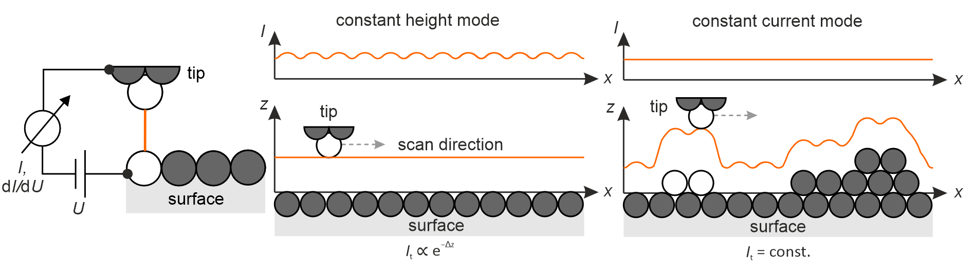
    Scanning Tunneling Microscopy (STM) enables the local investigation of structural and electronic properties in real space with atomic-scale resolution. Its operating principle relies on quantum mechanical tunneling: when a conductive tip is brought to a few ångström distances from a conducting or semiconducting surface and a bias voltage (typically 10 mV–2 V) is applied, electrons tunnel through the vacuum barrier. The resulting tunneling current I depends exponentially on the tip-sample separation and is highly sensitive to the local electronic density of states (LDOS). Consequently, STM can detect apparent height variations as small as a few picometres; such minute corrugations often arise from stress‑induced relaxations of the atomic lattice (or from local electronic effects). Observing individual surface atoms is straightforward, because they often appear as protrusions of roughly one ångström (≈ 0.1 nm), i.e., about two orders of magnitude larger than the picometre‑scale height variations that the STM can resolve. The extremely fine sensitivity of modern STMs enables even the most subtle changes in electronic structure to be detected.

    The two most commonly used imaging modes are:

    Constant Height Mode (CHM) – The tip scans at a fixed vertical position while the tunneling current I(x, y) is recorded. Changes in the current directly reflect variations in tip-sample distance and the local density of states. CHM is ideal for atomically flat surfaces or for monitoring fast dynamic processes (e.g., surface diffusion), but requires extremely stable conditions to maintain the constant tip height.

    Constant Current Mode (CCM) – A feedback loop continuously adjusts the tip height to keep the tunneling current constant as the tip scans laterally. The recorded height profile z(x,y) therefore maps the surface topography combined with variations in the local electronic density of states. Because the tip height is actively regulated, CCM is well suited for rough or highly corrugated samples, as it reduces the risk of destructive collisions between the tip and the sample.


  • © AG Schlenhoff

    Scanning Tunneling Spectroscopy (STS)

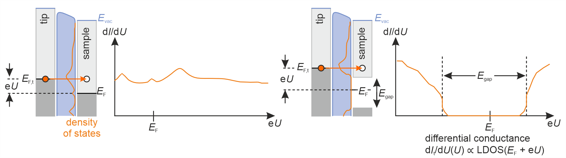
    Scanning Tunneling Spectroscopy (STS) - STM is not only a tool for imaging surfaces; it can also be used as a spectroscopic probe of the electronic structure with atomic‑scale spatial resolution and meV‑ or even µeV‑energy resolution (depending on the instrument configuration). The principle relies on the fact that the differential conductance dI/dU is proportional to the local electronic density of states (LDOS) of the sample at any chosen energy.

    In a typical scanning tunneling spectroscopy (STS) measurement the tip is positioned over a point of interest, the feedback loop is switched off, and the sample bias U is swept while the current I is recorded. The conductance spectrum, dI/dU(U), can be obtained in two ways: either by numerically differentiating the measured I(U) curve, or, more commonly, by adding a small sinusoidal modulation (usually 1–20 mV rms at a few kHz) to the bias voltage, then demodulating the resulting AC component with a lock‑in amplifier; this yields dI/dU directly.

    The resulting dI/dU curve reflects the LDOS at each bias voltage (corresponding to an energy E = EF + eU ). For instance, the Shockley surface state on Au(111) appears as a step at about –0.5 eV, while the band gap of a semiconductor shows up as a region of vanishing conductance within the gap. Because the tip can be moved with atomic precision, STS maps the spatial evolution of these electronic features and can be combined with the topographic image obtained in constant‑current mode, allowing a direct correlation between structure and electronic properties.

    Inelastic Tunneling Spectroscopy (IETS) - Beyond the elastic tunneling channel, electrons can lose energy e.g. by exciting vibrational, phononic, or magnetic modes of the sample. These inelastic tunneling channels contribute only a few percent of the total current, making them invisible in the raw I(U) signal. Their presence is revealed as a subtle step in the first derivative and, more prominently, as a peak (or dip) in the second derivative d2I/dU2.

    IETS is performed with the same lock‑in setup used for STS, but the lock‑in output is demodulated at the second harmonic of the modulation frequency to obtain the second derivative. Typical energy scales range from a few meV for magnetic spin excitations to tens of meV for surface phonons and up to a few hundred meV for molecular vibrations.

    Consequently, IETS enables the study of single‑molecule vibrational modes, the spatial investigation of phonons in moiré heterostructures, and the detection of collective spin excitations such as magnons in magnetic samples. By combining the elastic information provided by STS with the inelastic insights from IETS, the microscope delivers a comprehensive picture of both the static electronic structure and the dynamic excitations of a surface, all with atomic‑scale spatial resolution.


  • © AG Schlenhoff

    Resonant Tunneling

    Image‑potential states (IPSs) as local quantum sensors - In addition to conventional STM/STS, the microscope can be operated in a resonant‑tunneling (field‑emission) mode. In this configuration the electron tunneling from the tip to the surface is mediated by image‑potential states (IPSs), which act as intermediate quantum states residing in the vacuum gap. As the IPS is located in front of the surface, it can sense aspects of the sample that are invisible to conventional tunneling.

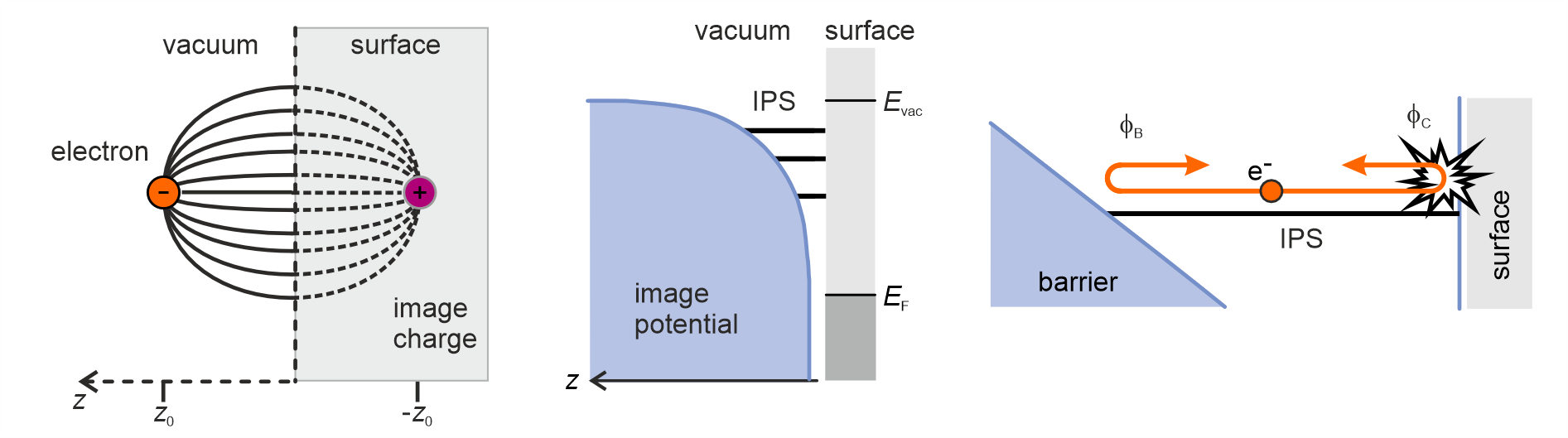
    The origin of IPSs can be understood as follows. When an electron approaches a polarizable surface it induces a polarization charge in that surface; this effect can be represented by a virtual image charge of opposite sign (left schematic in figure above). The resulting Coulomb‑like attraction creates a potential well in front of the surface (center schematic). Within this well a discrete series of Rydberg‑like bound states— the IPSs—evolve. An electron occupying an IPS is effectively confined by repeated reflections between the surface and the vacuum barrier, accompanied by respective phase shifts of the electron’s wave function upon reflection (right schematic). In the phase‑accumulation picture, a stable IPS forms when the sum of the phase shifts satisfies a quantization condition.

    Because of this electron reflection from the surface, the IPS is extremely sensitive to the unoccupied electronic band structure at that energy and to atomic‑scale variations in the scattering potential. Reflection at the vacuum barrier makes the IPS equally sensitive to the shape of the barrier itself; thus any lateral variation that modifies the electrostatic potential in front of the surface—such as a local charge transfer at a buried interface and/or a work‑function change—shifts the IPS energy.


    © AG Schlenhoff

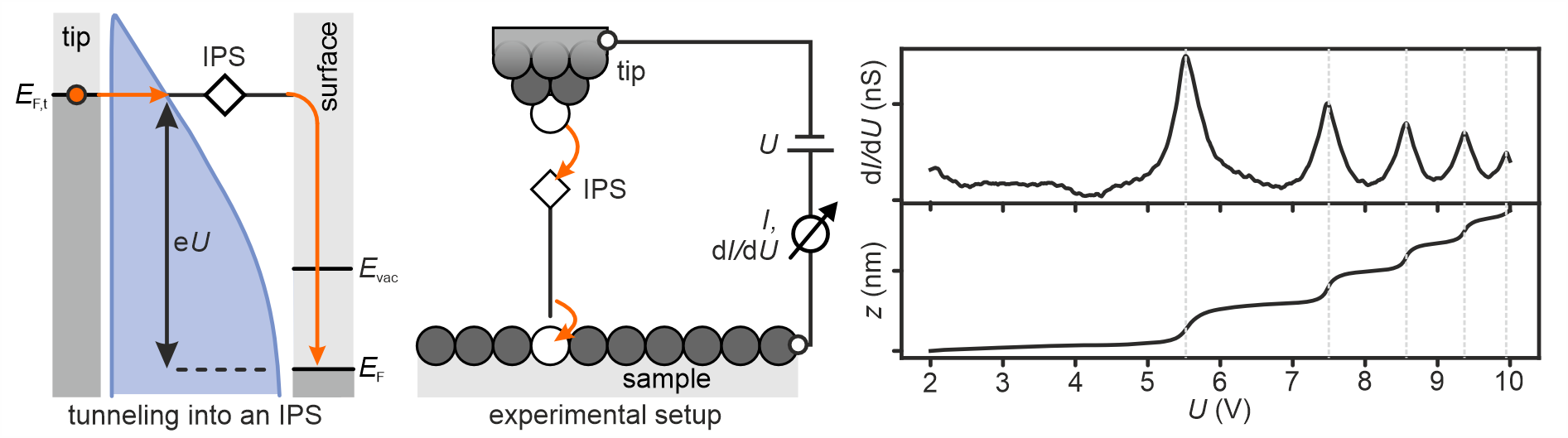
    Resonant Tunneling - Within an STM, IPSs can be probed with ultimate spatial resolution. This is realized in the field emission (or resonant tunneling) mode, i.e. when the applied positive bias eU exceeds the sample work function (left schematic). The electric field between tip and sample Stark‑shifts the IPS series to higher energies and expands them. By tuning the bias voltage, individual IPSs can be selectively addressed.

    In order to identify the IPSs, STS is typically performed in constant current mode. The feedback loop keeps the current constant by adjusting the tip height z while the bias U is ramped. For eU larger than the work function the current is dominated by Fowler–Nordheim field emission. Consequently, the loop maintains roughly a constant electric field at the tip, which forces the tip to retract as U increases (right panel). As depicted in the left panel, when the tip’s Fermi level aligns with an IPS energy, electrons tunnel resonantly through that state. The resonant channel sharply increases the transmission probability, producing a peak in the differential conductance dI/dU(U). Accordingly, the tip has to retract overproportional to compensate for the additional transmission channel, resulting in a step in the tip-sample displacement z(U) . Typical dI/dU(U) and z(U) curves revealing the first five members of the IPS series are displayed in the right panel.

    By scanning the tip, local variations in IPS energy can be mapped and correlated directly with the structural, electronic and magnetic information obtained from conventional (spin-polarized) STM/STS. Because of their special nature (described above) IPSs provide access to surface properties that are unattainable with conventional STM/STS. For example, IPSs enable (i) mapping of the spin-dependent electron phase shift upon reflection at a non-collinear magnetic surface, (ii) sensing of the spin density at buried interfaces that are covered by non-magnetic passivation layers, and (iii) resolution of sub-surface structural changes in layered moiré heterostructures that remain invisible in direct tunnelling.

  • © AG Schlenhoff

    Spin-polarized Scanning Tunneling Microscopy (SP-STM)

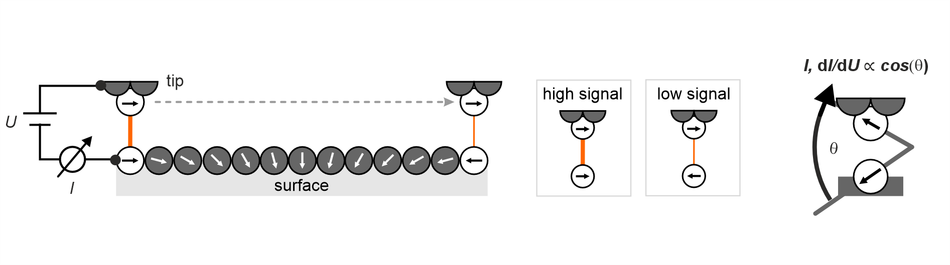
    In Spin‑polarized Scanning Tunneling Microscopy (SP‑STM) the spin dependence of the tunneling current I and of the differential conductance dI/dU between a magnetic tip and a magnetic sample is exploited to probe the local magnetic properties of a surface. Both quantities vary as the cosine of the angle θ between the tip magnetization and the sample magnetization. Consequently, a parallel alignment (θ = 0°) gives a maximal signal, whereas an antiparallel alignment (θ = 180°) yields the minimal signal. By raster‑scanning the probe tip with fixed magnetization direction and recording the spatial variation of either I or dI/dU, SP‑STM maps the surface spin texture with atomic‑scale resolution.

    Spin‑polarized Scanning Tunneling Spectroscopy (SP‑STS) is typically carried out while a small, reversible external magnetic field (B= ± 1 T) is applied. The field is used to align a soft‑magnetic tip (or to switch the magnetization of a soft‑magnetic sample), thereby allowing to deliberately set parallel and antiparallel configurations and to extract the spin‑dependent contribution to the tunneling signal. Under these conditions, SP‑STS reveals the effective spin polarization of individual electronic states and, when the states are spin‑split, the magnitude of that splitting.

    Thus SP‑STM provides a real‑space image of magnetic domains, domain walls, spin spirals, or magnetic skyrmions, while SP‑STS yields information on the spin‑dependent electronic structure that underlies those textures.

    External control parameter - In addition to probing intrinsic magnetic properties of a sample, SP-STM/STS offers a set of external knobs that can be used to perturb the magnetic system—whether it is in its ground state or a metastable configuration—and to study its response. These knobs include static magnetic fields, tip-sample electric fields of adjustable magnitude and polarity, spin polarized currents that can be varied over several orders of magnitude, and controlled variation of the base temperature. By tuning any of these parameters and recording the resulting changes with SP-STM/STS, the magnetic behavior can be explored systematically under well defined external stimuli.


  • © AG Schlenhoff

    Light-Assisted (LA-)STM/STS

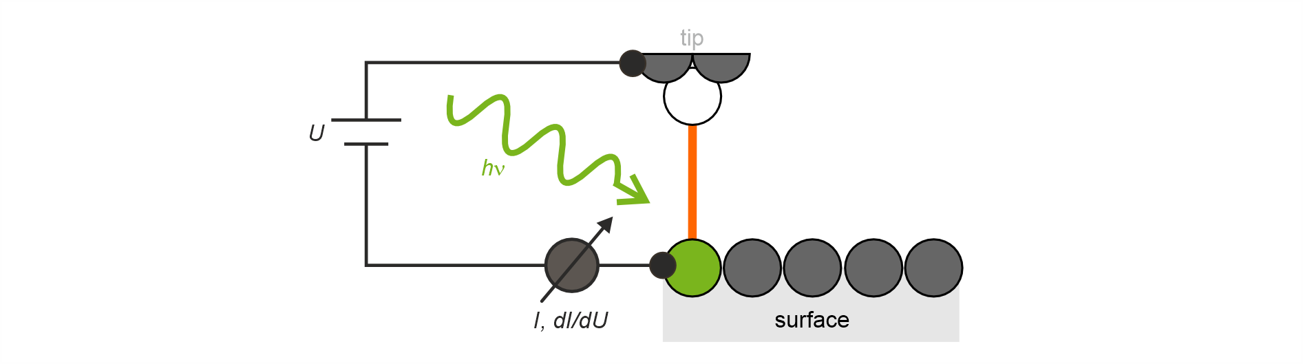
    In Light‑Assisted Scanning Tunneling Microsopy and Spectroscopy (LA-STM/STS) the tunneling junction is illuminated while the microscope operates in its usual STM or STS mode. Photons of energy ℏω that strike the surface promote electrons from occupied states (e.g., the valence band or the Fermi level) into higher‑lying unoccupied states such as the conduction band, image‑potential states, or excitonic levels. This photo‑induced population change, together with any accompanying band‑gap renormalization, modifies the tunneling current I and the differential conductance dI/dU, so that LA‑STS spectra contain new or shifted features that are absent in the dark. Because the tip can be positioned with sub‑ångström precision, these optically induced electronic signatures can be mapped with atomic‑scale spatial resolution and directly correlated with the structural and electronic information obtained from conventional STM/STS under dark conditions, thus revealing, for example, how local defects, adsorbates, or strain influence the photo‑response.

    Two measurement approaches are typically used. In the first, the same area of the sample is investigated once with the laser blocked (light off) and once with the laser unblocked (light on); the difference between the data sets reveals the effect of photo‑excitation on the local electronic structure. In the second, the laser intensity is amplitude‑modulated (continuous‑wave or pulsed) while the STM electronics remain in differential‑conductance mode; a lock‑in amplifier referenced to the modulation frequency extracts the light‑induced component of the tunnelling signal, providing a highly sensitive detection of the photo‑response.

    LA‑STS enables the study of processes that are initiated by photons — e.g., charge carrier generation, exciton formation, transient band‑gap renormalization, and other light‑driven phenomena — that would not occur in an all‑electronic tunneling experiment. By combining optical excitation with the unrivalled spatial precision of tunneling microscopy, light‑assisted STM/STS opens a window onto photon‑induced processes at the single‑atom level while retaining the atomic‑scale imaging and spectroscopy capabilities of conventional STM.


  • In-situ Molecular Beam Epitaxy (MBE)

    Molecular Beam Epitaxy (MBE) is a thin‑film deposition method that grows crystalline layers atom by atom under ultra‑high‑vacuum (UHV) conditions. For this technique, the constituent elements—typically supplied from heated effusion cells—evaporate and form highly collimated molecular beams that travel unimpeded to a substrate held at a precisely controlled temperature. Because the mean free path of the atoms exceeds the dimensions of the chamber, the beams reach the surface without scattering, allowing the material to arrange itself directly onto the crystal lattice of the underlying layer.

    By opening and closing shutters on each source, individual monolayers can be added in a precisely timed sequence, producing abrupt interfaces and complex multilayer structures such as quantum wells and heterojunctions. Sub‑monolayer coverages can also be achieved, yielding nanostructures that are only one atomic layer high. When two or three elements are co‑evaporated, binary or ternary compounds can be fabricated in situ by reactive growth.

    The combination of an atomically clean environment, low growth rates, and precisely controlled deposition yields films of exceptional purity and structural perfection, making MBE indispensable for the investigation of well‑defined experimental model systems.