PEEM experiments
In our workgroup we are studying the charge and energy transfer processes of organized organic adsorbates, e.g. organic dyes on (oxidized) SiC. To understand the interplay between the adsorbates and the substrate as well as interactions between the adsorbates the lifetimes of occupied and unoccupied states of different organic complexes can be investigated. These organic adsorbates are not uniformly distributed over the surface, but tend to form islands of different aggregations. These islands exhibit slightly different electronic configurations, therefore leading, for example, to different lifetimes of excited states.
We have already successfully functionalized SiC substrates with several organic dyes by wet chemistry as well as evaporation in vacuum and characterized these by inverse photoemission, X-ray photoelectron spectroscopy, and fluorescence microscopy, the latter confirming distinguishable sites of agglomerations of the organic dyes.
Measurements of the lifetimes of unoccupied states are normally carried out by two-photon photoemission (2-PPE). Since classical 2-PPE spectroscopy does not yield any spatial information, the recorded signal integrates over the complete light spot on the sample. Therefore it is impossible to conclude the lifetimes of different structures from the measurement.
To overcome this limitation the 2-PPE set-up for such samples needs to provide a spatially resolved signal, which can be achieved by using an electron microscope. This type of microscope is called photoemission electron microscope (PEEM). Fig. 1 shows a scheme of a typical setup: The sample is connected to ground to prevent it from charging. Electrons that are emitted from the sample by incident light are then accelerated by an electrode with up to 16 kV, the so called extractor. Sample, extractor, the focus electrode and the column act together as the equivalent to an objective lens in an optical microscope. They image the electrons emitted from the sample into the image plane of the two electrostatic projective lenses, which in turn magnify the intermediate image. Astigmatisms resulting from lens errors of the electrostatic lenses can be compensated by the stigmator, an octopole electrode.
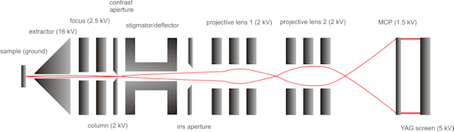
Fig. 1: Schematic representation of a typical PEEM-setup, the voltages correspond to the maximum voltage of each part of the PEEM; the red line denotes the electron path.
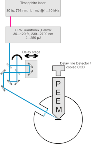
In our experiments we use an optical parametric amplifier (OPA) pumped by a Ti:Sa laser with pulse energies up to 1.1 mJ, a pulse duration of 30 fs and repetition rates between 1 and 10 kHz. The OPA is gaplessly tunable from 230 nm to 2700 nm with pulse durations between 30 fs and 120 fs and pulse energies between 2 µJ and 250 µJ, depending on the desired output wavelength. A motorized delay stage with a Michelson-type interferometer splits the resulting pulses in two and introduces an adjustable delay with femtosecond resolution.