Research
The research of the nanoelectronics group focuses on emergent and interaction driven phenomena of two-dimensional quantum materials, two-dimensional charge carrier systems, related hetero-, and hybrid structures as well as interfaces. The aim is to gain a fundamental understanding of the physical properties of those systems, and to learn – in a next step – to control and tailor them on purpose with the vision to achieve novel functionalities and at the same time to look for potential application in an interdisciplinary context. These low-dimensional systems are therefore integrated in nano- and microscale circuitries, as well as in proof-of-concept and prototypical devices to explore their potential for opto-/electronic or energy harvesting applications and to serve as test-bed structures towards quantum technologies.
We pursue our scientific goals with modern optical and electronic experimental techniques at extreme cryogenic environments reaching temperatures lower than 10 Millikelvin. Our research interests are clustered around the following directions that are detailed below:
a. Excitons in 2D materials: From correlated ensembles to deterministic quantum light sources
b. Mott-Hubbard physics and correlated phases in twisted vdW bilayerss
c. 2D polar metals: Novel atomically thin quantum and meta materials
d. Emergent phenomena in low-dimensional quantum systems
e. Van der Waals hetero- and hybrid stacks for energy conversion application
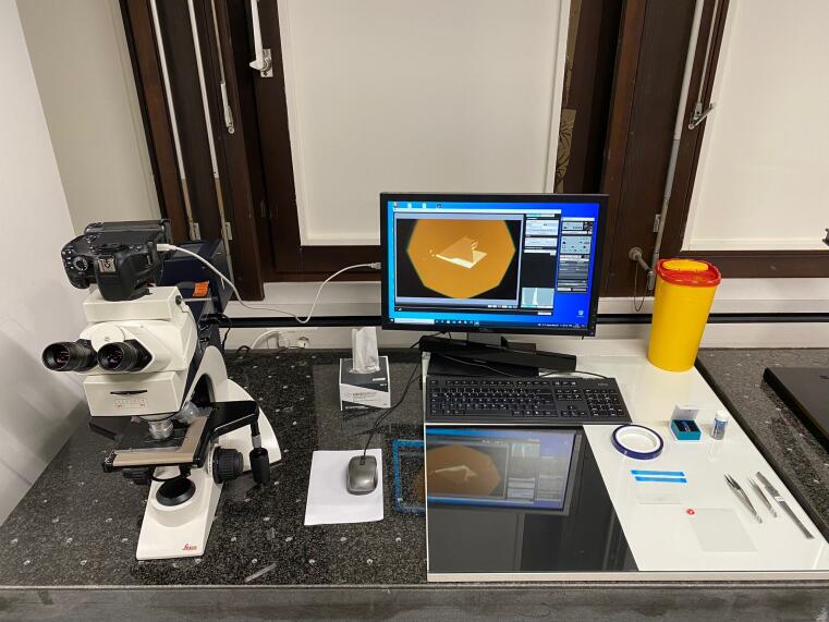
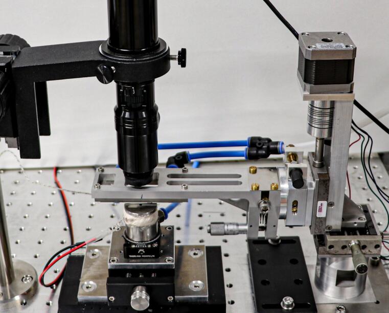
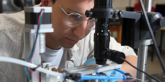
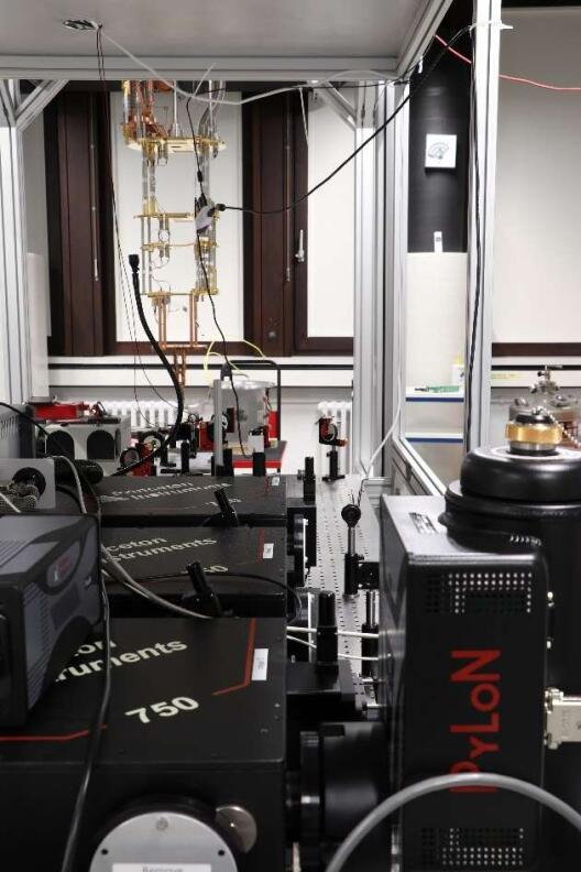
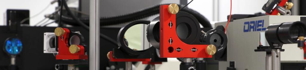
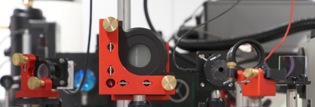
g. Optical Characterization Labs
a. Excitons in 2D materials: From correlated ensembles to deterministic quantum light sources
Exciton ensembles
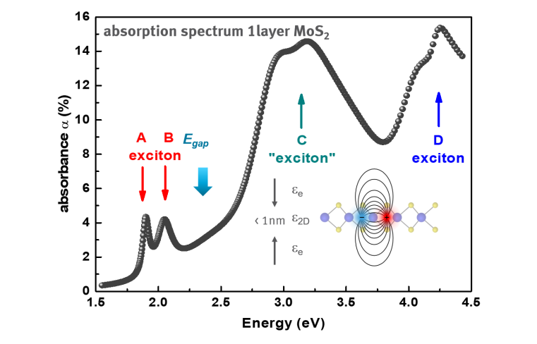
An exciton is a pair of electron and hole bound together by Coulomb interaction. Excitons are observed in the optical spectra of semiconducting 2D materials such as MoS2 and WSe2 which provide a natural analogue to quantum wells. Due to the two-dimensional nature and reduced screening of the Coulomb forces, the excitons in 2D materials are very strongly bound. Besides the intralayer excitons which reside in one layer, interlayer excitons exist in the heterostructures of 2D materials. Here the electron and hole reside in different layers due to type-II band alignment. This makes the excitons longer lived and imparts a permanent electric dipole moment. Such excitons are suitable to study interaction-driven many body phases such as Bose-Einstein condensate. Thus, excitons in 2D materials are suitable for both fundamental studies such as exciton condensation, as well as for applications in exciton-based devices such as excitonic lasers, transistors and modulators. The aim of our group is to investigate the fundamental properties and interactions of excitons in 2D materials and their heterostructures as well as to embed them in nanoscale devices and establish control of these properties.
Quantum light sources
Excitons in 2D materials can also be localized at at the moiré lattice sites that is formed in the 2D material heterostructures or deterministically positioned defect sites or. Scalable and deterministic SPEs are desirable for applications in modern information and quantum technologies. We established 2D materials as a scalable platform for single-photon emitters with unprecedented control of position as well as photophysical properties owing to the all-interfacial nature. On-demand creation and precise positioning of mono-typical single-photon sources in atomically thin MoS2 with very high fabrication yield is achieved by focused ion beam irradiation with helium ions. Atomistic defects with anti-bunched emission lines with sub-10 nm lateral and 0.7 nm axial positioning accuracy can be produced in already processed circuitries. We aim to invest the control of these quantum emitters by external stimuli such as electric fields and to implement them in (2D) plasmonic and opto-electronic circuitries towards real-world quantum applications, e.g. on-chip quantum networks.
b. Mott-Hubbard physics
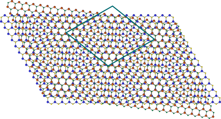
The Hubbard model is used in theoretical physics to calculate the behavior of electrons in a solid-state material. The model is based on a highly periodic lattice with one electronic state at each lattice site. The model takes a nearest neighbor hoping and an onsite repulsion by other electrons into account. Therefore, this model is suitable to describe strongly correlated systems that show correlated phases such as magnetism, superconductivity, Mott insulator and others. The Hubbard model, however, is theoretically only solvable for some one-dimensional systems. Experimentally, the Mott Hubbard models can be simulated in real physical system like ultracold atoms trapped in an optical lattice. Better experimentally accessible systems are solid states materials. However, the required nearly perfect highly modulation of the electronic structure is difficult to achieve. We overcome this issue by preparing twisted bilayers of two-dimensional crystals. Thanks to the van der Waals bonding between the atomically thin layer, two single layers of 2D materials can be stacked on top of each other with precisely controlled twist angel. Slightly different lattice constants and the twist angle result in a geometric superlattice structure, a Moiré lattice also known in digital photography. The moiré lattice provides the required highly periodic “lattice-like” modulation of the electronic band structure to simulate Mott-Hubbard physics in experiment. By controlling the doping and hence the filling factors of the moiré bands in such systems using an electronic gate, it is possible to demonstrate different correlated phases. We aim to study correlation phenomena in twisted and gated homo- and hetero-bilayers acting as Hubbard simulators by a combination of resonant inelastic light scattering, optical interband excitations as well as transport investigations at cryogenic temperatures.
c. 2D polar metals: Novel atomically thin quantum and meta materials
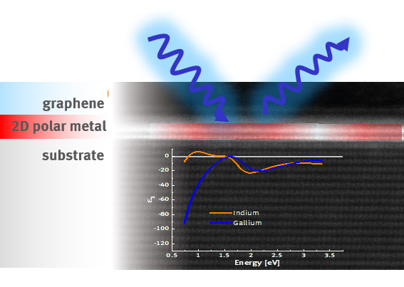
Key for optical technologies is the manipulation of the light-matter interaction to achieve a high level of control, particularly in technologically relevant solid-state nanomaterials. We study new and promising classes of atomically thin 2D polar metals such as 2D Ga, In, Ag, Sn and others, as well as their alloys. We work here in close collaboration with Prof. Robinson (Penn State) who has pioneered the growth if novel half-van der Waals materials. These quantum confined 2D metals exhibit fascinating properties like superconductivity, strong plasmonic responses, enormous nonlinear optical properties emerging by giant second harmonic generation and tunable epsilon near zero (ENZ) behavior qualifying them as metamaterials. Due to the half-van der Waals nature, we combine these 2D metals with other van der Waals materials with excitonic, spin or topological interesting properties in order to study coupling and proximity effects and to achieve novel functionalities. Their tunability and possibility for integration in van der Waals heterostacks makes 2D polar metals attractive systems for the realization of atomically thin metamaterials, quantum-confined metal films, tunable (quantum-)plasmonics and nano-photonics. We aim to explore the optical and transport behavior of those systems by a combination of spectroscopic imaging ellipsometry, transport and Raman measurements in order to explore their electronic and optical properties.
d. Emergent phenomena in low-dimensional quantum systems
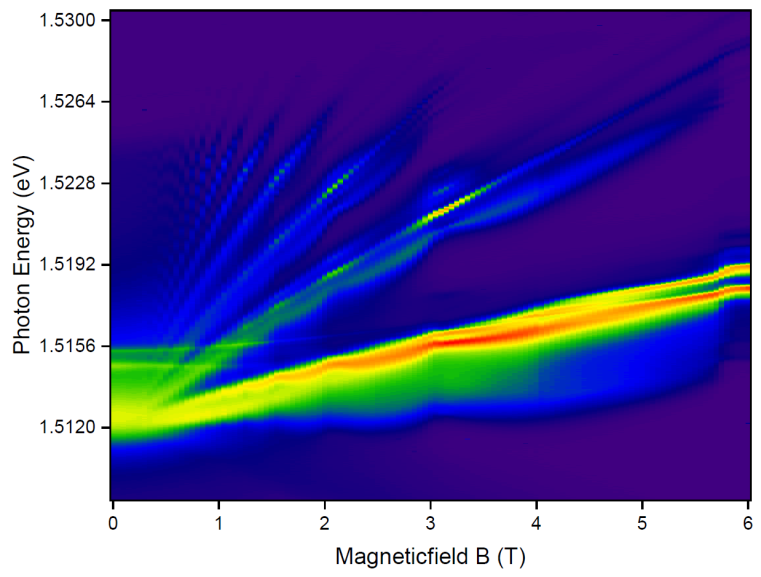
The physical properties of solid-state (quantum) systems are determined the particles and quasiparticles such as electrons, phonons (lattice vibrations), plasmons hosted by the solid as well as their manifold interactions. The light-matter interaction is for instance of great relevance for opto-/electronic materials, whereas electron-electron and electron lattice interactions are key in charge and heat transport processes. If the interactions strength is significantly enhanced and the quasiparticle behaves in a collective manner, those systems can show emergent behavior, e.g. superconductivity, magnetism, fractional quantum hall states, topological non-trivial states of matter and other correlated phases. Emergent phenomena are caused by interactions of many particles by intertwined degrees of freedom and are hence macroscopic phenomena that cannot be described by the properties of the individual constituent. The most important degree of freedoms in low-dimensional quantum systems that we are interested in are charge, spin, orbital, lattice and topology. We study spin-and orbital related phenomena as well as superconductivity in two-dimensional quantum materials and are interested in exotic, presumably non-abelian phases of matter of certain fractional quantum Hall effect states (FQHE) hosted in ultra-high mobility two-dimensional charge carrier systems in GaAs/AlGaAs heterostructures. Our aim is to generate a fundamental understanding of those fascinating emergent phases of matter. We research those phases by a combination of interband emission and absorption, spectroscopic ellipsometry, resonant inelastic light scattering and (magneto-)transport investigations at low temperatures.
e. Van der Waals hetero- and hybrid stacks for energy conversion via (photo-)catalysis
To power our today’s life style, alternative “green” energy conversion and storage strategies are important, but the efficiency is still low. Efficient energy conversion processes including photovoltaics, (photo-)catalysis or thermoelectrics requires a fundamental understanding of the underlying mechanisms at the solid-solid and solid-liquid interface. We mainly focus on the development of a microscopic understanding of light-matter interaction, charge transfer processes, interfacial phonon coupling and heat transfer in realistic device schemes or under reaction conditions. As an example, we developed an electrochemical microcell with all optical access to study in operando optical interband transitions and phonon processes with sub-micrometer resolution identifying the dominant catalytically active sites in MoS2 mono- and multilayers to be edges and point defects on the basal plane. With this knowledge, we developed a strategy to increase the catalytic activity by additional point defects. Moreover, we use solid and liquid electrolytes as gate electrodes and are interested in the cross-plane charge and heat transport towards thermoelectric applications.
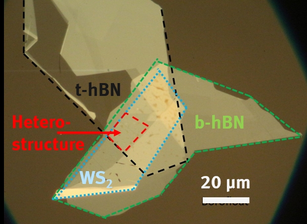
f. Hybrid superconducting-2D semiconductor systems for optically tunable neuromorphic computing
Neuromorphic computing aims to emulate the functionality of biological neural networks with energy-efficient hardware systems. Josephson junctions (JJs), particularly those based on high-temperature superconductors, offer ultrafast operation and inherently low power consumption, making them promising candidates for future neuromorphic architectures. However, a key missing component remains the implementation of an integrated and tunable memory element. We explore novel hybrid devices that couple high-TC superconducting materials such as YBa₂Cu₃O₇ (YBCO) with semiconducting two-dimensional materials like WS₂. These 2D materials serve as optically active gate elements, enabling external light-based control over the critical current IC of the junction via photodoping effects. Our approach aims at achieving reversible, non-volatile memory states governed by optical stimuli, paving the way towards all-optically controlled superconducting logic. The hybrid structures are fabricated using van der Waals stacking techniques and are characterized by a combination of Raman and photoluminescence spectroscopy, spectroscopic ellipsometry, and photocurrent measurements to gain insights into the charge transfer dynamics and interfacial coupling mechanisms.
This project has received funding from the European Union's Horizon Europe research and innovation program under grant agreement No 101130224 'JOSEPHINE'.