
Fundamentals of Nanofabrication
The course Fundamentals of Nanofabrication is a practical tutorial within the modules "Functional Nanosystems" and "Quantum- and Nanotechnology" that form part of the Master studies in Physics at the WWU Münster. The tutorial is offered at the end of every semester as a 7 full working day block course and has a maximum capacity of 15 students per semester. We recommend timely registration by following the information given in QISPOS (please observe the deadlines for course inscriptions set by the university).
Parts of this course were also offered within the "Laboratory Course PolyNano" at the Department of Chemistry and Pharmacy every other semester but cannot currently be offered in this format anymore.
The course imparts basics skills in modern nanofabrication and -characterization techniques through research-oriented teaching and learning. The applied methods are similar to those used both in the semiconductor industry for manufacturing state-of-the-art electronic integrated circuit as well as in the emerging field of nanophotonics where light is guided in nanoscale dielectric structures on a silicon chip.

Goals of the Course
In this lab course the students develop a basic understanding of how nanoscale integrated structures are realized and acquire first-hand experience with modern nanofabrication processes. During this course, the students fabricate three different samples with techniques which are also commonly used in the semiconductor industry, as for example spin coating, magnetron sputtering and photo and electron beam lithography. The students learn how to operate all tools under the supervision of a trained supervisor, and they study the parameters of the fabrication and their effect on the results.
In the first part, the students fabricate a nanoscale temperature sensor. After this first section, the students have the skills to clean samples using solvents and sonication and to coat samples with photo resist using a spin coater. Furthermore, they are capable of performing photolithography using a mask aligner and they are able to develop photo resist in a developer. In addition, they know the influence of the process parameters, as for example spin coating speed, spin coating duration, exposure time and development time. Finally, the students understand how to take images using scanning electron microscopy and how to improve the image quality.
In the second part, the students fabricate a fully functional organic light emitting diode (OLED). This section aims to consolidate the knowledge and skills the students have acquired in the first section. In addition, the students are capable of fabricating a multi-layer sample. Furthermore, they understand the working principle of an OLED.
In the third part, the students fabricate a nano pattern of their own choice (see information below). This part focuses on writing a pattern with an electron beam. After this section, the students are capable of coating a sample with electron beam resist using a spin coater and developing it after the exposure. Most importantly, the students know the working principle of electron beam lithography (EBL) and its differences and similarities to photolithography. They are able to write a pattern with EBL under the supervision of a trained supervisor.
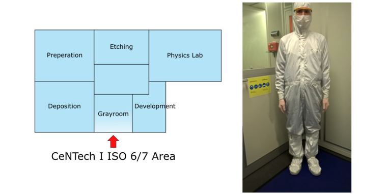
In the field of nanofabrication, contamination due to particles can damage the structures on a sample. For this reason, a clean environment is required, which is provided by a cleanroom. Most of the equipment used in this lab course is located in a state-of-the-art clean room that forms part of the Münster Nanofabrication Facility (MNF) at the Center for Nanotechnology (CeNTech). Such an environment is essential not only for nanofabrication but also finds its application in medical and biological science, laser technology and many other research fields. After the lab course, the students know how to enter, work and behave in a cleanroom.
Prerequisites
Students are expected to have basic knowledge in experimental physics (e.g. as acquired in laboratory courses I & II within the Bachelor studies in Physics at the WWU Münster) and - most importantly - be highly motivated! A very significant aspect of the course is concerned with working in a cleanroom environment. Working in a cleanroom is both a challenge and a privilege that is usually reserved to a selected group of specially trained experts. Within the course, students will work alongside the research staff at highly technical and expensive equipment, which forms the backbone of one of the core profile areas at the University of Münster with top-level research activities in nanoscience. This requires the students' physical ability and cooperation for strictly complying with standard clean room procedures in order to guarantee the safety of all users as well as preserving the working conditions (i.e. avoid contamination of the clean room). While safety protocols and code of conduct form part of the training, students should be aware that all activities inside the clean room will necessarily involve wearing special garments (see pictures below) and the use of personal protective equipment.


Organization
The course comprises 13 exercises, each consisting of an experiment of approx. 3 hour duration. The participants will work in groups of 2-3 students. Due to the limited capacity of the cleanroom and the availability of the tools we can only accommodate one group at a time. Typically groups start on a Monday and follow the below schedule. The maximum number of groups is limited to 5 per semester such that the maximum number of participants is limited to 15 students per semester. Groups will be formed in the organizational meeting (for date, time and location see the course overview / Vorlesungsverzeichnis (QISPOS)) where also the starting dates will be assigned. To successfully complete the course (and thus collect the credit points) all experiments need to be completed and each groups needs to hand in a (joint) report no later than 6 weeks after having finished the last experiment.
Before the organizational meeting, all students should enroll for the course on the Learnweb (see QISPOS for further information), where also the literature and the instructions for the fabrication will be posted. At the beginning of each day, the literature required for that day will be discussed.
Pictures and Phrases for Electron Beam Lithography
During the lab course the students will fabricate a chip with a pattern and a QR code (a word or phrase) of their choice. For this pattern the students should send a digital photo with sizes 100x100px, 150x150px, 200x200px and 250x250px along with the phrase to the course organizer (to be announced during the organizational meeting) a few days before their first day of the lab course. Before sending the pictures, these should be converted into black-white with removed background. Some good examples are shown below.
Exercise 1 - Spincurves
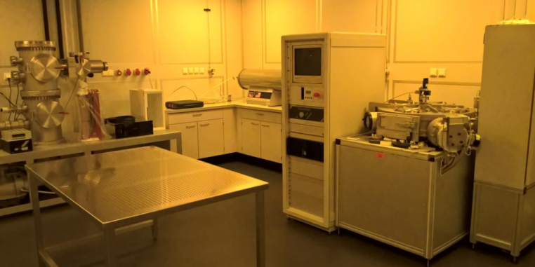
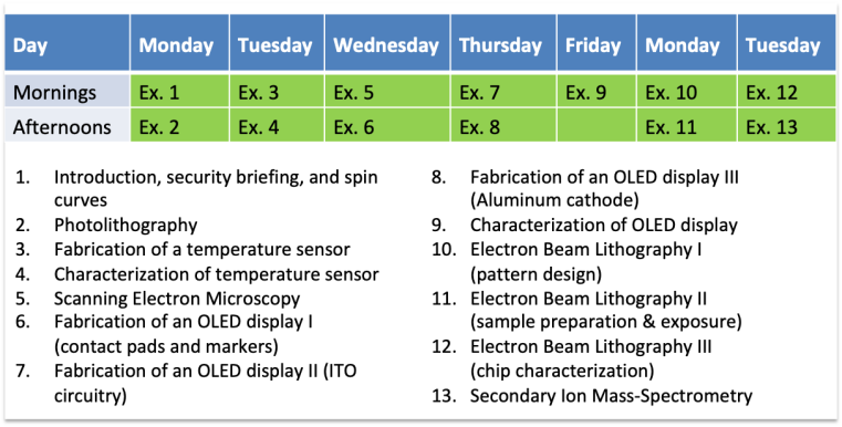
In the first exercise, the students measure a spin curve for photo resist. They spin photoresist on a sample using a spin coater as shown in the image below. Finally, the resist layer is characterized using a film thickness measurement instrument. Here, students learn how to clean samples using solvents in combination with sonication and subsequent dehydration on a hotplate. In addition, they learn how to use a spin coater and they study the influence of the settings on the result.
Solvent bench for sample preparation© MNF 
Spin coater© T. Grottke Exercise 2 - Photolithography
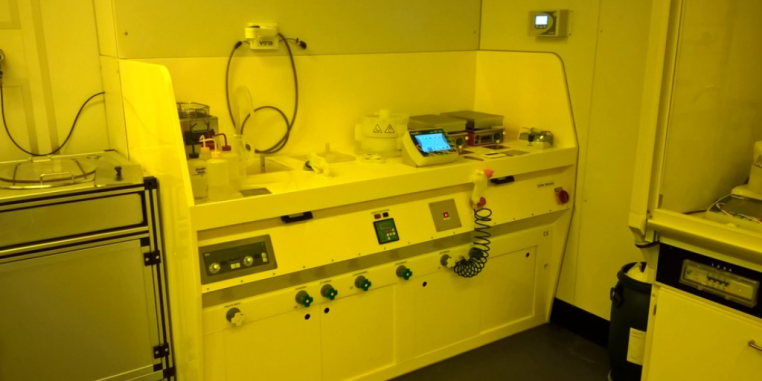
In the second exercise, the students expose resist-coated samples in a photolithography tool. This exercise includes studying the operation of the tool, the reaction of photoresist to exposure with UV-light und the development after the exposure. Afterwards, the students use an optical microscope to investigate the final samples. The pattern transfer from a photomask to the samples is performed on a mask-aligner that operates conceptionally very similar to lithography systems used in the semiconductor industry (see images / video below).
Wafer (click for video)© Micron Technology, Inc. 
Maskaligner© T. Grottke 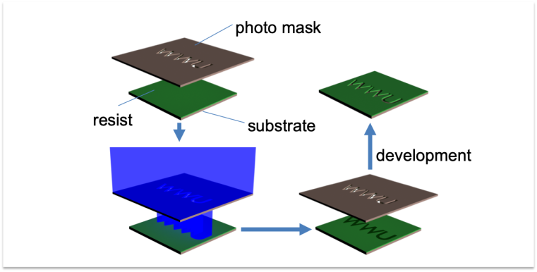
Photolithography process© T. Grottke Exercise 3 - Temperature Sensor Fabrication
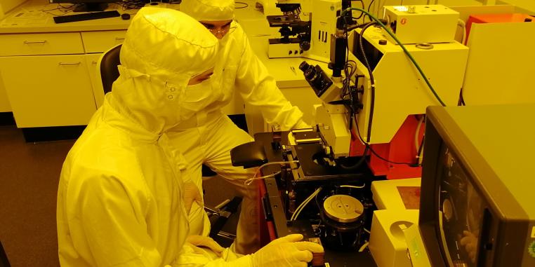
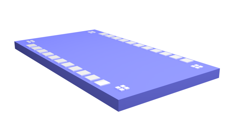
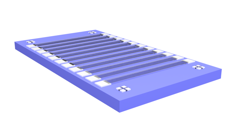
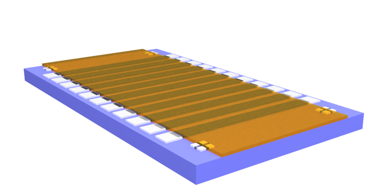
In the third exercise, the students fabricate a temperature sensor. This sensor consists of different aluminium wires with different lengths and widths on a silicon platform (see picture below). To fabricate this sample, in addition to spin coating, photolithography and development, the students carry out a magnetron sputtering process. This is a process to deposit materials, in this case aluminium, on a sample. After the development, parts of the chip are still covered by photoresist. This resist along with the aluminium on this resist are removed in a lift-off process. In this exercise, the students learn how to use a magnetron sputter deposition tool, study its working principle and learn how to perform a lift-off.

Temperature sensor chip© T. Grottke 
Magnetron sputter deposition tool© T. Grottke 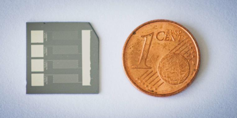
Temperature sensor chip next to a coin© J. Schütte Exercise 4 - Temperature Sensor Test
In the fourth exercise, the students characterize the performance of their temperature sensors. The resistances of different wires are measured. To characterize the temperature dependency of the resistances, this measurement is carried out at different temperatures, including a measurement in liquid nitrogen. In this exercise, the students examine the behavior of conductors and semiconductors at different temperatures. In addition, the electrical properties of thin films are studied.

Measurement setup for the temperature sensor chip© F. Beutel Exercise 5 - Scanning Electron Microscopy
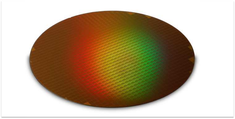
In the fifth exercise, the students investigate the fabrication quality of the temperature sensor chip using scanning electron microscopy. This tool allows for a high resolution so that possible defects can be examined with a higher accuracy compared to an optical microscope. The students study the working principle of a scanning electron microscope, learn how to operate this tool and how a good image quality can be achieved.
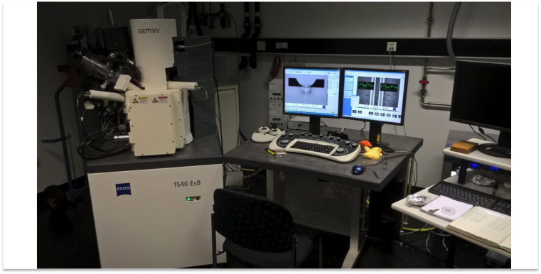
Scanning electron microscope© T. Grottke 
SEM micrograph of a temperature sensor chip© M. Wolff 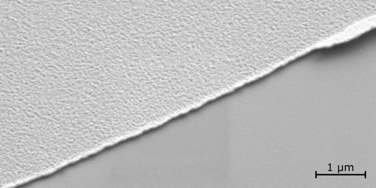
SEM micrograph of an aluminium wire© M. Wolff Exercise 6 - OLED Fabrication I
In the sixth exercise, the students fabricate the first part of a fully functional organic light emitting diode (OLED). The total fabrication consists of three exercises followed by an additional exercise in which the students analyze their sample. In this step, the students pattern the aluminium structures on glas samples with the nanofabrication techniques they learned and studied in the previous exercises. This exercise aims to consolidate the knowledge and skills the students have acquired during the first five exercises.
First step of the OLED: Aluminium pads and markers© T. Grottke Exercise 7 - OLED Fabrication II
In the seventh exercise, the students fabricate the anode (indium tin oxide, ITO) of the OLED using a spin coating process, photolithography, development and a magnetron sputtering process. The students acquire advanced mask aligner techniques. In particular, they learn how samples with several layers can be fabricated and how these layers can be aligned.
Second step of the OLED: ITO anodes© T. Grottke Exercise 8 - OLED Fabrication III
In this last fabrication step of the OLED, the sample is coated with MEH:PPV solved in Chloroform. This serves as active layer of the OLED. To finalize the OLED, a shadow mask is placed on the sample. After depositing aluminium on the sample, the shadow mask can be removed, leaving behind the cathode (aluminium). These wires are arranged perpendicularly with respect to the ITO wires, resulting in an OLED with 8 by 12 pixels.
Third step of the OLED: Active layer© T. Grottke 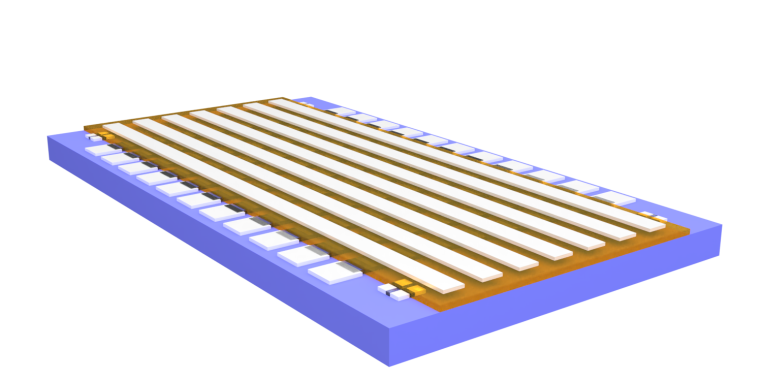
Fourth step of the OLED: Aluminium cathodes© T. Grottke Exercise 9 - OLED Test
In this exercise, the students take a closer look at their OLEDs. In particular, an I-V curve is measured using a voltage source. If the fabrication works, light emission will be visible. An optical microscope is used to analyze the sample before and after the measurement and the results, in particular possible defects and their reasons, are discussed.
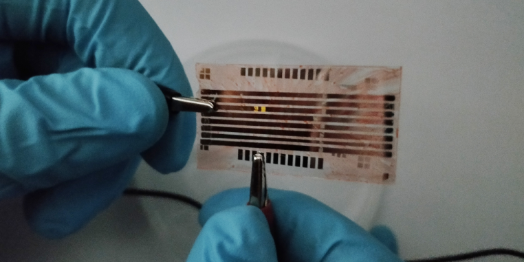
OLED emitting light© F. Beutel 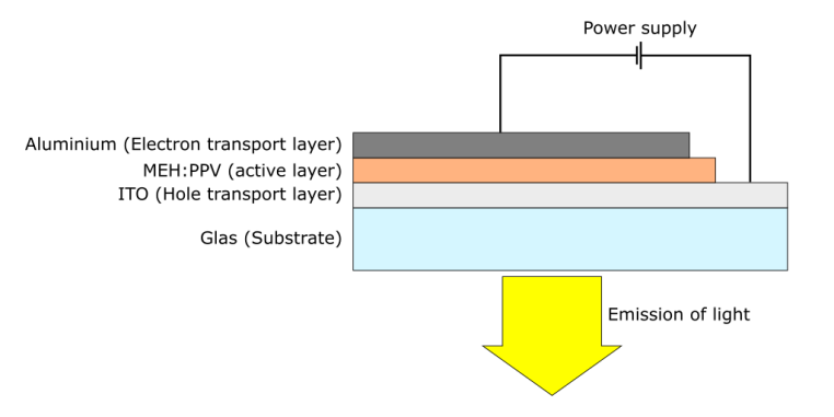
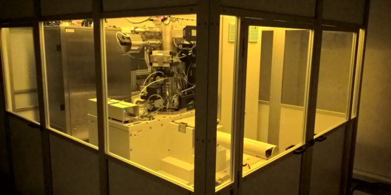
© T. Grottke Exercise 10 - Electron Beam Lithography Introduction
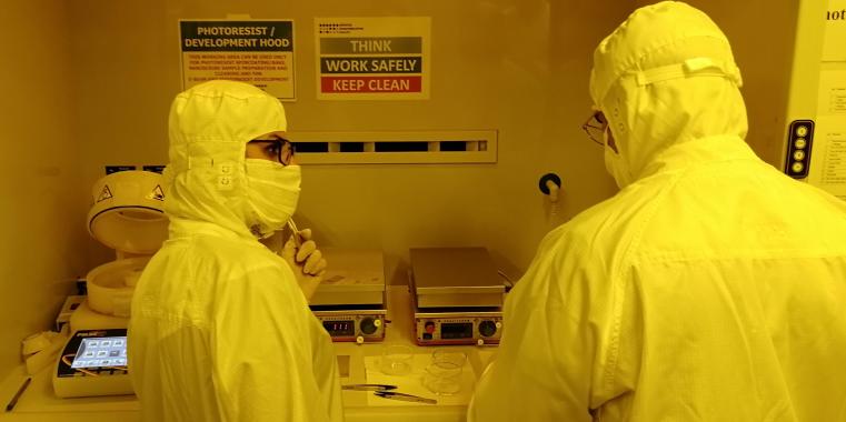
In this exercise, the students use electron beam lithography (EBL) to pattern a structure and a phrase of their choice on a chip (see inforrmations above). To fabricate the samples, silicon chips are coated with electron beam resist and subequently exposed using an electron beam. The exposure of the samples is perfomed with different doses so that the effect of under and overexposure can be studied. Before the actual writing, the students learn how their pictures and phrases are transferred to a file format which can be loaded at the EBL system.
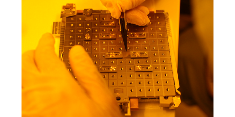
Chip on the sample holder© T. Grottke 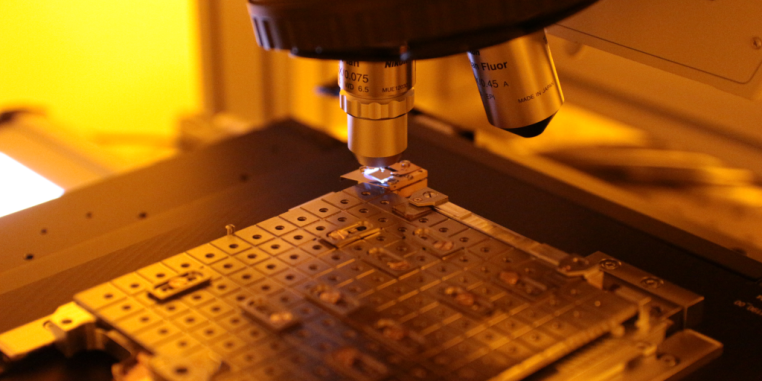
Chip on the sample holder© MNF Exercise 11 - Electron Beam Lithography Exposure
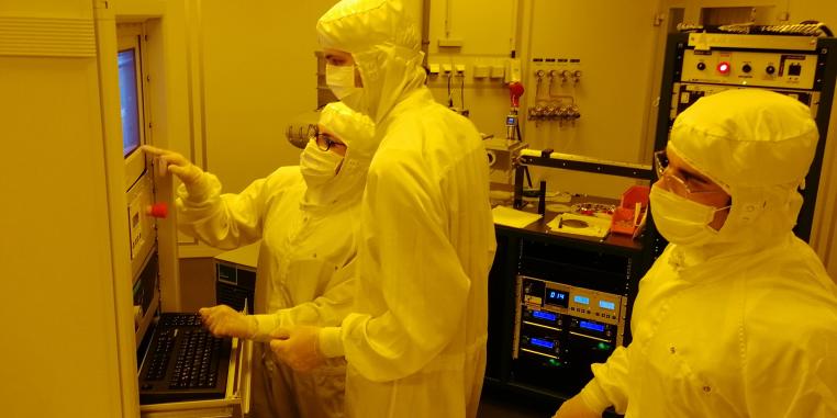
In this exercise, the samples are unloaded from the EBL system und subsequently developed. A magnetron sputtering process and a lift-off are performed to deposit aluminium on the sample and to subsequently remove the resist and parts of the aluminium, resulting in the finalized samples.
Electron beam lithography© MNF 
Electron beam lithography© MNF Exercise 12 - Electron Beam Lithography Characterization
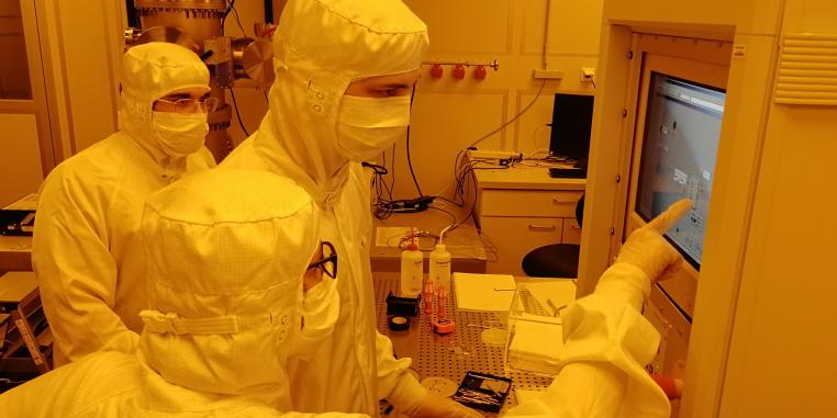
In this exercise, the students analyze their final samples using optical microscope and SEM. In particular, the influence of the dose will be studied in more detail. In addition, terms like under and overdosed and proximity effect are discussed on the basis of the fabricated samples.
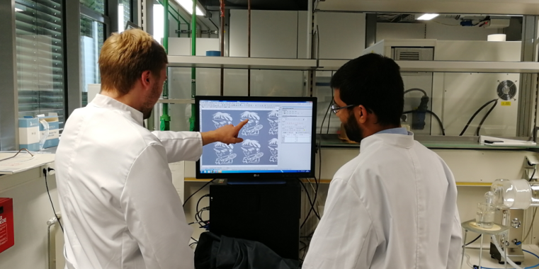
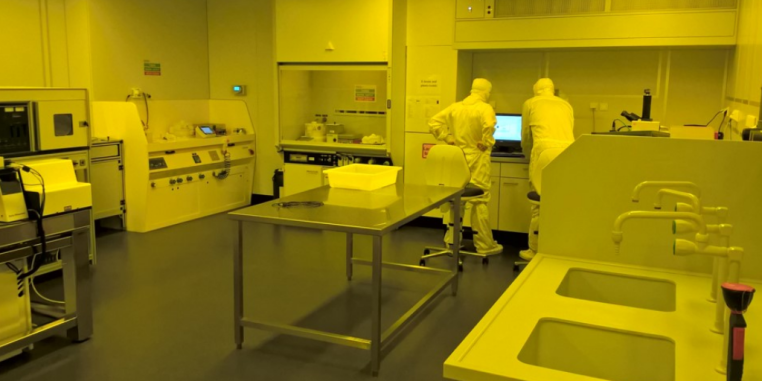
Students analyzing their EBL sample© T. Grottke Exercise 13 - Time-of-Flight Massspectrometry
This 13th and last exercise is performed in the laboratory of Prof. Arlinghaus and consists in using a Time-of-flight Secondary Ion Mass Spectrometer (Tof-SIMS) to characterize samples prepared in the previous exercises.
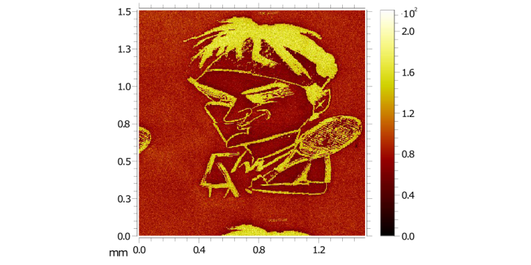
Federer© M. Heeger Lab Report Requirements
The lab report should be a self-standing and self-consistent document, allowing the reader to be able to reproduce the represented results.
The following structure could be used as a guideline for the report:- A brief introduction including the motivation of the lab course
- Fabrication process / Theory
Describe the working principle of the machines and tools you used without going to deep into the details. Also describe the theoretical background of the samples you are going to fabricate. - Fabrication of the samples
Describe the fabrication of your samples. Which machines and tools did you use and which settings did you choose? - Analysis/ Evaluating the fabrication process
In this chapter all measurement results and the taken microscope pictures should be presented and described. Do the measurements agree with the theory and your expectations? If no, why not? What do you see on the pictures? How do the settings of the fabrication influence the result? - Conclusion
Summarize what you did and learned during the lab course.
Try to formulate as compact and precise as possible. Avoid using terms like “… is very big/small” and give numbers or references instead. Explain previously unknown terms like “dose” or “over-exposure”. All microscope pictures should contain a scale bar. Pictures taken from somewhere else have to be cited. The report should in general include what you learned within the lab course.
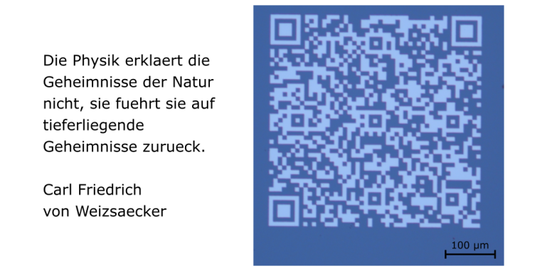
C.F. von Weizsäcker© T. Grottke 
Dr Who© T. Grottke 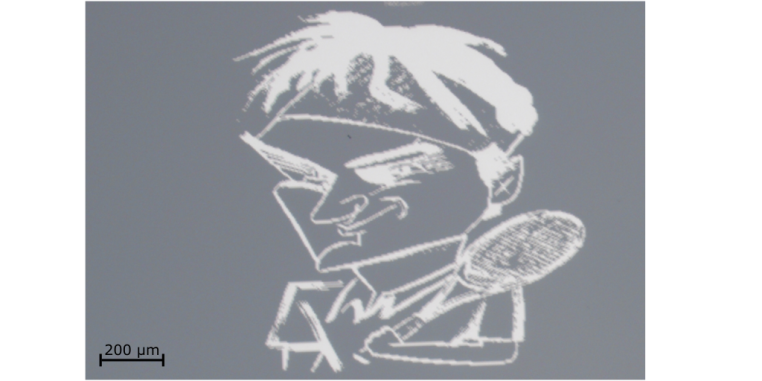
Federer© T. Grottke 
Sunshine© T. Grottke 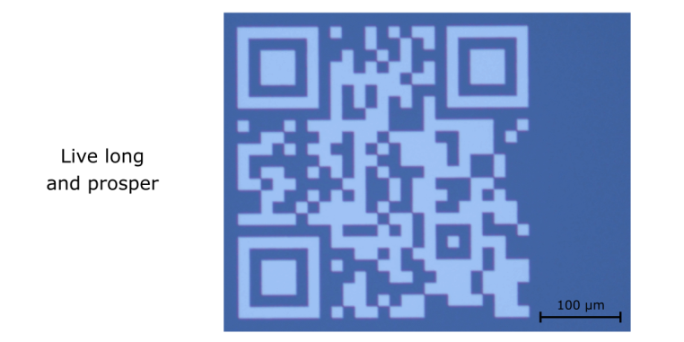
Live long and prosper© T. Grottke 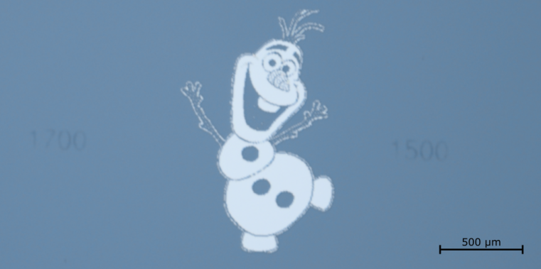
Snowman© T. Grottke 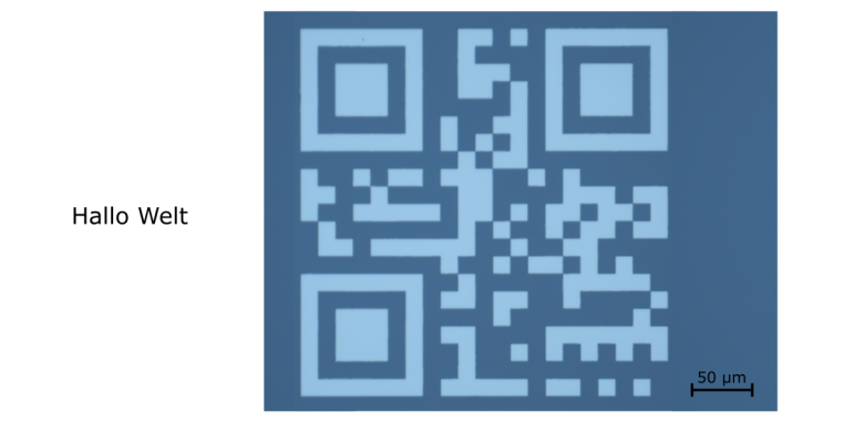
Hello World© T. Grottke 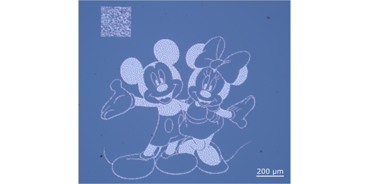
Mickey Mouse© T. Grottke