Engineering quantum nano-systems: functional defect sites
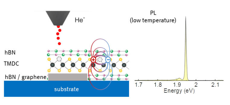
Scalable and deterministic single-photon emitters are desirable for applications in modern information and quantum technologies. We established 2D materials as a scalable platform for deterministic and addressable single-photon emitters with unprecedented control of position owing to their all-interfacial nature. On-demand creation and precise positioning of mono-typical single-photon sources in atomically thin semiconducting 2D materials with high fabrication yield is achieved by focused ion beam irradiation with helium ions. Atomistic defects with anti-bunched emission lines with sub-10 nm lateral and <8 nm axial positioning accuracy can be produced in already processed circuitries. We aim to investigate the control of these quantum light sources by external stimuli such as electric fields and to implement them in (2D) plasmonic and opto-electronic circuitries towards real-world quantum applications, e.g. on-chip quantum networks.
Engineered quantum nano-systems: emergent phenomena
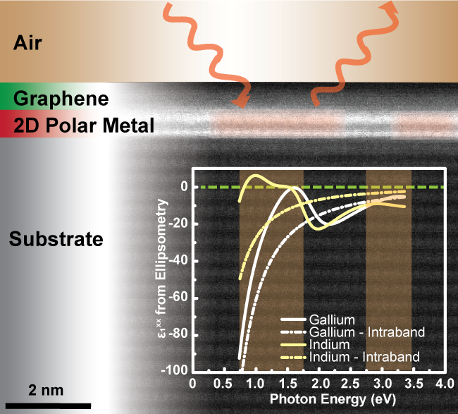
Important for all (quantum) optical technologies is the manipulation of the light-matter interaction to achieve a high level of control, particularly in technologically relevant solid-state quantum-nanomaterials. Atomically thin two-dimensional materials receive great interest in this regard because of their unique properties. Among others, a novel and promising class of atomically thin crystals are 2D polar metals such as 2D Ga, In, Ag, Bi as well as their alloys. Those quantum confined metals exhibit fascinating properties like superconductivity, strong plasmonic responses in the visible range and strong nonlinear optical properties emerging by giant second harmonic generation in the NIR range together tunable epsilon near zero behavior. Due to the half-van der Waals nature, we combine these 2D metals with other van der Waals materials to achieve novel functionalities. Their tunability and possibility for integration in van der Waals heterostacks makes 2D polar metals attractive for realizing quantum engineered metal films, tunable (quantum-)plasmonics and nano-photonics.