
Studies on the electronic structure of spatially aligned armchair graphene nanoribbons
Steffen Linden, Fabian Kleimeier
1. Introduction:
A decade ago the discovery of graphene, a graphitic film with a thickness of one atomic layer, was published, which has various mechanical, thermal and electronical benefits [1] (see also link zu Thorbens Seite). With a semi-metallic character caused by a zero band gap and a Dirac-conical linear dispersion relation at the k-point, two dimensional graphene is a promising material for various fields of application.
For electronic devices semiconducting materials play a prominent role. On the one hand functionalization of graphene by adsorption of hydrogen results in a bandgap opening in graphene [2]. On the other hand a limitation of the expansion of the graphene sheet in one dimension results in a measureable band-gap caused by quantum confinement of the electrons [3,4]. Further theoretical calculations predist a dependence of the band gap on the width of those graphene nanoribbons(GNRs) [5,6].
Our experimental investigations on one dimensional so called armchair GNRs (aGNRs) revealed a band gap of 2.6 eV for the 7aGNR molecule and 2.0 eV for the chevron-type [7].
2. Preparation and experimental setup:
Atomically precise, sub-nm broad armchair GNRs could be fabricated by on-surface reactions starting with a convenient primer molecule as it is shown in Figure 1(a), (b), receiving the 7-aGNR and the chevron-type aGNRs, respectively, following the synthesis scheme performed at first by Cai et al. [8].
Spatially aligned 7-aGNRs and chevron-type aGNRs could be aprepared on a stepped Au(788) substrate, which is observed by STM and shown in Figure 1 (a),(b)).
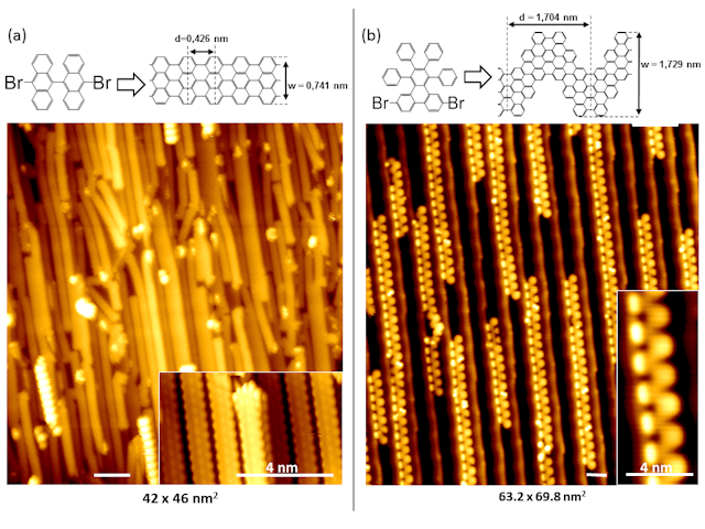
Figure 1: Synthesis scheme for (a) 7-aGNR and (b) chevron type aGNR. The STM pictures below show the
parallel alignment of both molecules along the substrate’s steps
Electronic investigations of the aGNR samples were performed by ARUPS (Angle Resolved Ultraviolet Photoelectron Spectroscopy), where electrons are excited from the molecular orbitals by irradiation with UV light via the photoelectric effect (see Fig 2 (a)).
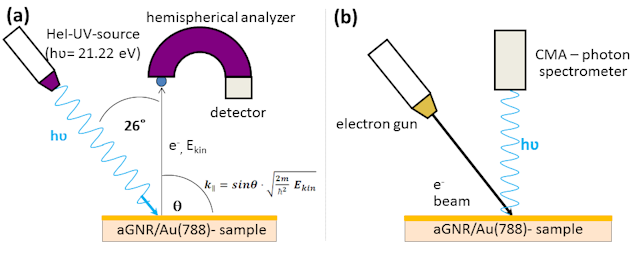
Figure 2: Schematic experimental setup for observing occupied states via ARUPS (a)
and the unoccupied states via IPE (b)
For both, the 7-aGNR and the chevron-type aGNR molecule, ARUPS was performed in an angular range of -40° and +40° relative to the detector axis. IPE (Inverse Photo Emission) measurements could be performed just in normal emission at the Γ-point. All spectra, which are obtained this way by ARUPS and IPE, were separated from its background by subtracting spectra of the pure substrate Au(788) as well.
3. ARUPS and IPE results:
Analysis of the spectra yields states at -0.7 eV and -1.2 eV (below the Fermilevel) showing a weak angular parabolic dispersion indicated by blue and red dots (see Fig 3(a)). In IPE measurements states at 0.7 eV, 1.9 eV, 3.3 eV, 4.4 eV for the 7-aGNRs can be observed. The origin of the relatively weak feature at 0.7 eV above the Fermilevel is not clarified, but the signal might be originated from quantum-dot like behaviour of fused ribbons of varying width, or from an interface state of the Au(788) substrate.
For the chevron-type aGNRs states were observed at -0.7 eV, -0.9 eV and at -1.8 eV and -1.9 eV as well (see Figure 3(b)). Corresponding IPE spectra yield unoccupied states at 1.3 eV and 2.6 eV above the Fermilevel.
From the energetic difference the highest occupied molecular orbital (HOMO) and the lowest unoccupied molecular orbital (LUMO) the band gaps at the Γ-point can be estimated to EGap,7-aGNR =(2.6±0.4) eV for the 7-aGNR and EGap, chevr =(2.0±0.4) eV for the chevron-type aGNRs.
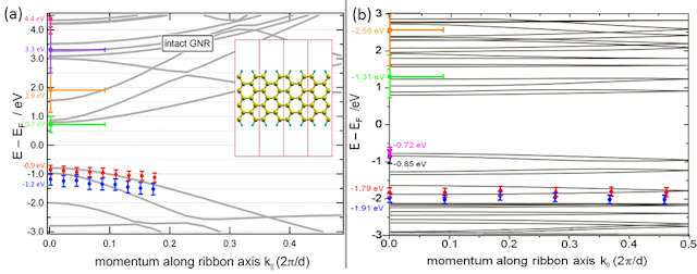
Figure 3: Energetic position of occupied states and unoccupied states for the 7-aGNR molecule (a) and the
chevron-type aGNR molecule (b) in colored points in comparison to band structure calculation
via LDA.
Many theoretical calculations were performed on those molecules applying LDA (local density approximation) and LSDA (local spin density approximation) to simulate the occupied and unoccupied states indicated by the black lines in Figure 3 (a),(b).
The comparison of the measured states to the calculations (Figure 3 (a),(b)) show good agreement for the position of the single states for both the 7-aGNR and the chevron-type aGNRs. Theoretically a band gap of about 1.6 eV is expected for the chevron-type aGNR (Figure 3(b)).
For the 7-aGNRs LDA calculations obtain a bandgap of ELDA=1.6 eV showing a noticeable deviance from the measured value (Figure 3(a)). Further calculations accounting for electron- electron interaction by GW-(Greens-Function) approximations yield a band gap of EGW=3.8 eV for the 7-aGNR [5,6], which is too much compared to the measured band gap.
The calculations are all done for pristine isolated aGNRs. The interaction of the GNR molecule and the substrate, on the other hand, results in screening of the electrons at the interface, thereby reducing the electron-electron interaction and thus minoring the band gap [9,10]. By this interpretation the weak feature at E= 0.7 eV above the Fermilevel could be assigned as a MIGS (metal induced gap-state) [11].
The direct experimental measurement of a band gap opening at the ?-point of one-dimensional aGNRs has been performed for the first time by ARUPS and IPE, so that the semiconducting character of aGNRs was verified experimentally.
4. Two– and three photon photoemission experiments on 7 aGNRs on Au(788):
Another, less ambiguous experimental method to measure unoccupied states is multiphoton-photoemission spectrocscopy. Here, the unoccupied state is first occupied by a photon with a photon energy that is smaller than the work function of the sample: hν<ΦA second photon is then absorbed by the electron in the previously unoccupied state and the electron is excited further, either into another unoccupied state or, if the photon energy is sufficient, into the vacuum.
Utilizing the second harmonic of a femtosecond Ti:Sapphire laser amplifier at 390 nm, we were able to identify two unoccupied states which overlap at around E-EF = 3.7 eV by three-photon photoemission (see Figure 4). The energetic position of the unoccupied states could also be reproduced by two-photon-photoemission with wavelengths between??=395nm and ?=285 nm (h?=3.95..4.35 eV).
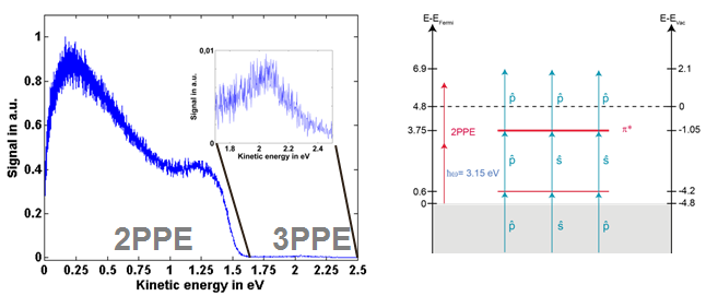
Figure 4: a) Photoemission signal from 7-aGNRs on Au(788) excited by laser pulses centered at 390nm. Inset: magnification of the 3PPE region. b) Resulting energy level diagram indicating different pathways to the unoccupied state.
By splitting the pulses at 390nm in two replicas in an interferometer and rotating the polarization of one of them by 90° to prevent interference effects, it is possible to measure the lifetime of the unoccupied state by delaying the two pulses with respect to each other. Integrating the signal over the energetic region of the 3 PPE signal then yields a convolution of the laser pulse duration with the exponential decay of the number of electrons in the excited state.
Experiments were carried out with pulse durations of 20 fs, a spot size of 300 µm and 50 nJ and 100 nJ pulse energy for the p-polarized and the s-polarized replica, respectively. When integrating over different parts of the 3 PPE signal, two different lifetimes can be observed depending on the energetic position of the integration, which indicates the presence of two different states being present. For integration over E-EF= 3.1..3.6 eV a lifetime of τ=100 fs is derived, whereas for integration over E-EF=3.6..4.25 eV a lifetime of about τ=85 fs is observed (See figure 5).
Repeating these measurements at different emission angles along the long ribbon axes to check for an influence of the impulse k|| on the electron dynamics of the states yielded no observable difference of the lifetime.
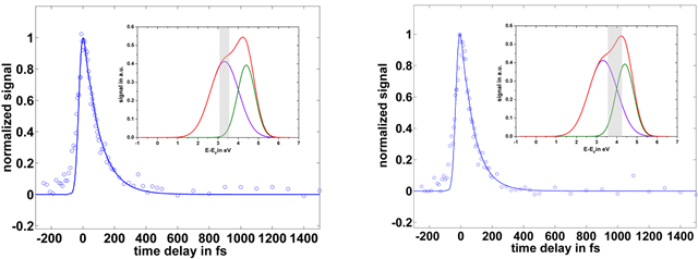
Figure 5: Time resolved signals integrated over different energetic regions of the 3 PPE signal. Insets: relevant part of the IPE data with the integration area greyed. Circles: measured, line: fit to the data. Negative delay means p-polarized pulse first.
a) E-EF=3.1…3.6eV with a lifetime of about ?=100 fs. b) E-EF=3.6…4.25 eV with a lifetime of about ?=80 fs.
5. Outlook:
- The origin of interaction of the GNRs and the substrate can be clarified by performing ARUPS and IPE on several stepped substrates like silver, copper, titanium,…. . It is expected, that the IPE feature at 0.7 eV above Fermilevel is varying in its energetic position and integral. Also the lifetimes are expected to depend on the substrate used as the energetic position of states affects the lifetime.
- Contamination dependent measurement by adsorption of gases (H2, O2,…) would clearify the effect of pollution on the electronic properties of the aGNRs. Similar calculations were published [12].
- Measurement of the electron dynamics of unoccupied states for other GNRs (e.g. chevron type on Au(788)) to check for the influence of the geometry and dimensions of the GNRs on the lifetime.
References:
[1] A. K. Geim et al. Nature Materials 6, 183-191 ( 2007)
[2] R. Balog et al., Nature Materials 9, 315–319 (2010)
[3] K. Nakada et al. Phys. Rev. B 54, 17 954-17961 (1996)
[4] M. Ezawa et al. Phys. Rev. B 73, 045432 (2006)
[5] Y.-W. Son et al., Phys. Rev. Lett. 97, 216803 (2006)
[6] D. Prezzi et al., Phys. Rev. B 77, 041404(R) (2008)
[7] S. Linden et al., Phys. Rev. Lett. 108, 216801 (2012)
[8] J. Cai et al., Nature (London) 466, 470 (2010)
[9] P.Ruffieux et al., ACS Nano 6, 6930–6935 (2012)
[10] L. Liang et al., Phys. Rev. B 86, 195404 (2012)
[11] C.Archambault et al., ACS Nano 7, 5414–5420 (2013)
[12] A. Fathalian et al., Physica B 417, 75–78 (2013)