
A
Advanced Functional Materials Vol. 11, No. 3 (2001)
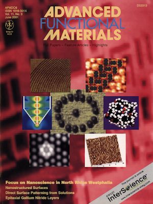
This issue of Advanced Functional Materials contains a representative collection of papers resulting from the research initiative "Nanoscience in North Rhine Westphalia"
H. Fuchs and G. Schmid
Research Initiative "Nanoscience in North Rhine Westphalia"
Adv. Funct. Mater. Vol.11, No.3, 167-168 (2001)
J. Poppensieker, C. Röthig and H. Fuchs
Investigation of the Epitaxial Growth of Octamethylene-Tetrathiafulvalene (OMTTF) on Substrates of Different Chemical Reactivity.
Adv. Funct. Mater. Vol.11, No.3, 188-192 (2001)
A. Schäfer, C. Seidel and H. Fuchs
LEED and Optical Spectroscopy Study of an Organic Epitaxial Multilayer Film.
Adv. Funct. Mater. Vol.11, No.3, 193-197 (2001)
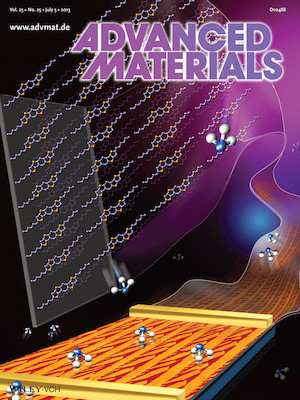
Advanced Materials Vol. 25, Iss. 25, p. 3419 (2013)
Liqiang Li, Peng Gao, Martin Baumgarten, Klaus Müllen, Nan Lu, Harald Fuchs and Lifeng Chi
High Performance Field-Effect Ammonia Sensors Based on a Structured Ultrathin Organic Semiconductor Film
Gas sensors based on organic field-effect transistors (OFETs) may enable a broad range of monitoring applications. Downscaling of organic semiconductor (OSC) films, in both vertical and lateral dimensions, is an efficient way to realize high performance OFET-based sensors, which is however technologically challenging. In this work we demonstrate a controllable growth of ultrathin microstripes with only 4-6 molecular layers (6.5-11 nm in thickness) of an OSC via dip-coating method. The ammonia gas sensing property of these untrathin microstripes is tested with OFETs geometry, which exhibits high sensitivity (INH3-off/INH3-on > 70 at 50 ppm NH3), fast response/recovery rate (several to tens of seconds), good selectivity, low detection limit, and reliable reversibility as well as stability. Such a performance represents a great progress in the field of OFET-based sensors. The result may promote the applications of OFETs-based sensors for low-cost, fast, and portable electronic nose.

Advanced Materials Vol. 25, Iss. 12, p. 1682 (2013)
Yuekun Lai, Fei Pan, Cong Xu, Harald Fuchs and Lifeng Chi
In Situ Surface-Modification-Induced Superhydrophobic Patterns with Reversible Wettability and Adhesion
Herein is described a facile, in situ, ink-regulating approach to rapidly achieve reversible water wettability and adhesion transition, with a large degree of contrast, on superhydrophobic TiO2 nanotube array film. The ink printing and removal process allows the wettability and reversible adhesion transitions to be realized. Experimental results demonstrate the potential application of such site-selective, sticky superhydrophobic patterns for droplet manipulation by in situ surface modification.
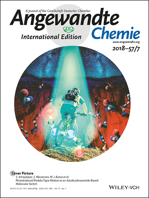
Angewandte Chemie International Edition Vol. 57, Iss. 07, p. 1723 (2018)
S. Amirjalayer, A. Martinez-Cuezva, J. Berna, S. Woutersen and W. Buma
Photoinduced Pedalo-Type Motion in an Azodicarboxamide-Based Molecular Switch
Well-defined structural changes of molecular units that can be triggered by light are crucial for the development of photoactive functional materials. Herein, we report on a novel switch that has azodicarboxamide as its photo-triggerable element. Time-resolved UV-pump/IR probe spectroscopy in combination with quantum-chemical calculations shows that the azodicarboxamide functionality, in contrast to other azo-based chromophores, does not undergo trans–cis photoisomerization. Instead, a photoinduced pedalo-type motion occurs, which because of its volume-conserving properties enables the design of functional molecular systems with controllable motion in a confined space.
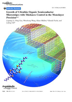
Angewandte Chemie International Edition Vol. 52, Iss. 48, p. 12530 (2013)
Liqiang Li, Peng Gao, Wenchong Wang, Klaus Müllen, Harald Fuchs and Lifeng Chi
Growth of Ultrathin Organic Semiconductor Microstripes with Thickness Control in the Monolayer Precision
Organic semiconductors: Growth of ultrathin (<15 nm), continuous, and microstructured organic semiconductor (OSC) films at monolayer precision is important for organic electronics and a challenging task. Uniform monolayer to hexalayer (ca. 1.6–12 nm; see picture) dendritic OSC microstripes at monolayer precision are grown by a dip-coating process.
Angewandte Chemie International Edition Vol. 52, Iss. 14, p. 3777 (2013)
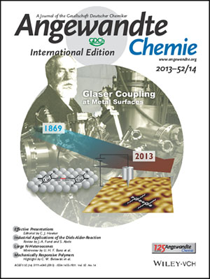
Hong-Ying Gao, Hendrik Wagner, Dingyong Zhong, Jörn-Holger Franke, Armido Studer and Harald Fuchs
Glaser Coupling at Metal Surfaces
On-surface synthesis enables the construction of defined nanostructures directly at surfaces through the covalent coupling of suitable organic precursors. These processes are carried out under ultrahigh-vacuum conditions and are monitored by scanning tunneling microscopy. In their Communication on page 4024 ff., A. Studer, H. Fuchs, and co-workers present a systematic study of the homocoupling of alkynes (Glaser coupling) as a versatile strategy for the construction of conjugated polymers at various metal surfaces.
Angewandte Chemie International Edition Vol. 123, Iss. 31, p. 7156 (2011)
Dingyong Zhong, Filipa Lourosa Sousa, Achim Müller, Lifeng Chi and Harald Fuchs
A Nanosized Molybdenum Oxide Wheel with a Unique Electronic-Necklace Structure: STM Study with Submolecular Resolution
A nanosized metal oxide wheel of the molybdenum blue type of polyoxometalates, the discovery of which was considered as a step to new length scales, has been studied by STM. In their Communication on page 7018 ff., A. Müller, L. Chi, H. Fuchs, and co-workers report that the Mo154 cluster has a unique compartmentalized electronic structure, in which each compartment contains two delocalized electrons. This discovery allows a better understanding of these species.
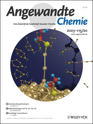
Angewandte Chemie Vol. 115, Iss. 20, p.2301 (2003)
Daniel Krüger, Roger Rousseau, Harald Fuchs and Dominik Marx
Mechanochemistry
... is the use of mechanical forces to induce and control molecular reactions. This link between chemistry and nanophysics is illustrated by D. Marx et al. on page 2251 ff. in a theoretical study: thiolate molecule is employed to stretch a gold cluster into a nanowire. The cover picture follows clockwise the isomerization steps that occur under the application of an external pulling force, such as that exerted by an atomic force microscope.
C
Chemical Physics and Physical Chemistry Vol. 2, Iss. 3, p. 187 (2001)
Michael Gleiche, Lifeng Chi, Erk Gedig and Harald Fuchs
Anisotropic Contact-Angle Hysteresis of Chemically Nanostructured Surfaces
Spatially alternating wetting properties are needed in order to test predictions on droplet contact angles on such complex, non-homogeneous surfaces. An evaporating droplet on a mica surface with hydrophillic strips 0.2–0.3 μm wide, as shown in the picture, recedes smoothly in directions parallel to the strips but in “jumps” with a variable contact angle perpendicular to the strips.
E

European Journal of Organic Chemistry Vol. 2007, Iss. 1, p. 3 (2007)
Athanasia Böhmer, Jens Brüggemann, Astrid Kaufmann, Albena Yoneva, Sonja Müller, Walter Müller, Frank Vergeer, Lifeng Chi, Luisa De Cola, Harald Fuchs, Xiaoming Chen, Takateru Kubota, Yoshio Okamoto and Fritz Vögtle
Long chain-substituted and triply functionalized molecular knots-synthesis, topological chirality and monolayer formation
The cover picture shows at the center the long tail-substituted trefoil knot species synthesized and investigated in this publication. The three peripheric segments show on the upper left side the enantiomers of these topologically chiral compounds, on the upper right side the detected triply bridged double knot and on the bottom a schematical illustration of the obtained Langmuir–Blodgett films. Details are discussed in the article by F. Vögtle et al. on p. 45 ff.
J
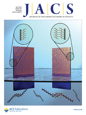
Journal American Chemical Society Vol. 132, Iss. 26, p. 8807 (2010)
Liqiang Li, Peng Gao, Klaus Schuermann, Stefan Ostendorp, Wenchong Wang, Chuan Du, Yong Lei, Harald Fuchs, Luisa De Cola, Klaus Müllen and Lifeng Chi
Controllable Growth and Field-Effect Property of Monolayer to Multilayer Microstripes of an Organic Semiconductor
This cover picture shows the controllable growth of partially aligned monolayer to multilayer micrometer stripes via dip-coating process. The number of molecular layers decreases with the increasing pulling speed. Lower pulling speed yields mixed multilayers (3-9 monolayers). It is noteworthy that pure monolayer and bilayer microstripes over large areas can be obtained at high pulling speed. The stripe morphology strongly depends on the pulling speed as well. XRD and confocal fluorescence measurements manifest that monolayer stripes are amorphous, while multilayer stripes (≥ 2) consist of crystalline states. FET devices were fabricated on these stripes. Monolayer stripes failed to reveal field-effect due to their amorphous state. In contrast, multilayer stripes exhibit good field-effect behavior. The controllable growth from monolayer to multilayer offers a powerful experimental system for fundamental research into the real charge accumulation and transporting layers for OFETs.
L
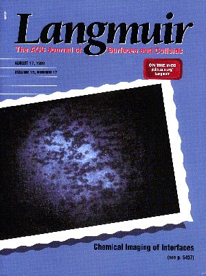
Langmuir Vol. 15, Iss. 17, p. 5437 (1999)
Mathias Flörsheimer, Christof Brillert and Harald Fuchs
Chemical Imaging of Interfaces by Sum Frequency Microscopy
We introduce a novel nonlinear optical microscope which provides interface specific, chemically and structurally resolved infrared information with the improved spatial resolution limit of a visible light microscope. High impact on the investigation of a large variety of interfaces is expected. Here, the microscope is applied in a dewetting study.
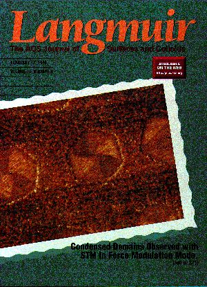
Langmuir Vol. 14, Iss. 4, p. 875 (1998)
Michael Gleiche, Lifeng Chi and Harald Fuchs
Study of Longe-Range Tilt Orientation in Fatty Acid Monolayers by Dynamic Scanning Force Microscopy
Segments in the liquid condensed (LC) domains of stearic acid, induced by long-range tilt orientation, were visualized on solid substrates by applying scanning force microscopy (SFM) using the force modulation mode (FMM). To understand the image contrast, a model based on the asymmetric apex of the SFM tip and the tilted phase of the molecules on the solid substrate after film transfer is presented. As a result, the apparent local elasticity is found to vary for molecules having the same tilt angle but different azimuthal angles. The observed textures are in good agreement with the theoretically predicted ones.
N
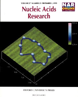
Nucleic Acid Research Vol. 27, Iss. 23, p. 4553 (1999)
Christof Niemeyer, Michael Adler, Bruno Pignataro, Steven Lenhert, Song Gao, Lifeng Chi, Harald Fuchs and Dietmar Blohm
Self-assembly of DNA-streptavidin nanostructures and their use as reagents in immuno-PCR
The self-assembly of bis-biotinylated double-stranded DNA and the tetravalent biotin-binding protein streptavidin (STV) have been studied by non-denaturing gel electrophoresis and atomic force microscopy (AFM). The rapid self-assembly reproducibly generated populations of individual oligomeric complexes. Most strikingly, the oligomers predominantly contained bivalent STV molecules bridging two adjacent DNA fragments to form linear nanostructures. Trivalent STV branch points occurred with a lower frequency and the presence of tetravalent STV was scarce. However, valency distribution, size and the exchange dynamics of the supramolecular aggregates were highly sensitive to stoichiometric variations in the relative molar coupling ratio of bis-biotinylated DNA and STV. The largest aggregates were obtained from equimolar amounts while excess STV led to the formation of smaller oligomers appearing as fingerprint-like band patterns in electrophoresis. Excess DNA, however, induces a complete breakdown of the oligomers, likely a consequence of the instability of STV conjugates containing more than two biotinylated DNA fragments. It was demonstrated that the oligomers can further be functionalized, for instance by the coupling of biotinylated immunoglobulins. Both pure and also antibody-modified DNA-STV oligomers were used as reagents in immuno-PCR (IPCR), a highly sensitive detection method for proteins and other antigens. Employment of the supramolecular reagents led to an approximately 100-fold enhanced sensitivity compared to the conventional IPCR procedure.
P
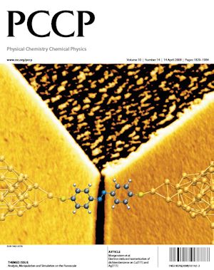
Physical Chemistry Chemical Physics Vol. 10, Iss. 14, p. 1829 (2008)
Harald Fuchs, Dominik Marx and Ulrich Simon
Analysis, manipulation, and simulation on the nanoscale
Research and development on the nanoscale has evolved to a wide-ranging and highly competitive field of research bridging the classical disciplines in molecule-based natural sciences, i.e. chemistry, physics, and biology.
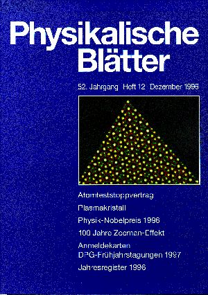
Physikalische Blätter Vol. 52, Iss. 12, p. 1241 (1996)
Jürgen Koglin, Ulrich Fischer and Harald Fuchs
Die Tetraedersonde - Optische Nahfeldmikroskopie mit 1 nm Ortsauflösung
Mit dem optischen Nahfeld-Rastermikroskop (englisch: Scanning Near Field Optical Microscope, SNOM) gelingt es, die beugungsbegrenzte Auflösung der Lichtmikroskopie zu umgehen. Meist wird eine zur Strahlung angeregte Öffnung (Apertur) an der Spitze eines metallbeschichteten transparenten Körpers als Sonde für das SNOM verwendet. Dabei stößt man aus technischen Gründen an eine Auflösungsgrenze bei 30 nm. Mit einer einfacher gestalteten, goldbeschichteten, tetraederförmigen Spitze als Sonde, die keine Apertur hat, gelang es jetzt, die Auflösung bis auf 1 nm zu steigern.

Physikalische Blätter Vol. 50, Iss. 9, p. 837 (1994)
Harald Fuchs
SXM-Methoden - nützliche Werkzeuge für die Praxis ?
Mit der Rastertunnelmikroskopie begann 1981 die Entwicklung einer großen Familie unterschiedlicher Nahfeld-Rastersondenmethoden, für die das englische Akronym SXM geprägt wurde. "S" steht hierbei für Scanning, "M" für Microscopy, und "X" steht alternativ für Tunneling, Force, Near field Optical, Near field Acustical, Ion Conduction, Thermal, etc. Oft werden die SXM-Methoden einseitig mit der Abbildung atomarer Landschaften assoziiert, die meist nur für die Grundlagenforschung von Interesse sind. Weitaus weniger bekannt sind die Möglichkeiten der SXM-Methoden in der anwendungsorientierten Forschung und Entwicklung, wo es auf die atomare bzw. molekulare Skala meist gar nicht ankommt. Welche Fragestellungen lassen sich denn nun erstmals mit diesen Techniken lösen oder zumindest effizienter lösen als mit konventionellen Methoden der (industriellen) Oberflächenanalytik?
S
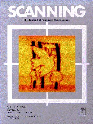
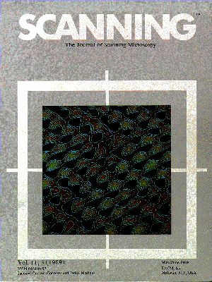
Scanning Vol. 18, Iss. 8, p. 567 (1996)
Andreas Naber, Holger Kock and Harald Fuchs
High Resolution Lithography with Near-Field Optical Microscopy
Scanning near-field optical microscopy (SNOM) is used for lithography to avoid the resolution limiting diffraction of conventional optical methods. We have expanded a commercial SNOM for writing even complex structures on the nanometer scale. Scanning near-field optical lithography (SNOL) has been applied to conventional resists to explore its potential and the possible combination with conventional optical lithography (mix and match technique).
Scanning Vol. 12, Iss. 3, p. 126 (1990)
Harald Fuchs and R. Laschinski
Surface investigations with a combined scanning electron-scanning tunneling microscope
We have combined a scanning tunneling microscope (STM) with a scanning electron microscope (SEM) for surface investigations of atomically flat surfaces, ultrathin adsorbate films, and material surfaces. The mechanical stability of the hybrid instrument allows high-resolution SEM of samples mounted on the STM stage and atomic resolution with the STM. Experimental results of combined SEM/STM investigations on textured material surfaces, submicron structures, and atomically flat conducting surfaces are presented. An example is given for surface machining with the STM under SEM control.
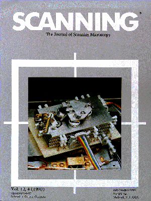
Scanning Vol. 11, Iss. 3, p. 139 (1990)
Harald Fuchs, W. Eustachi and R. Seifert
A data acquisition and image processing system for Scanning Tunneling Microscopy
We have built a dedicated data acquisition and image processing system for scanning tunneling microscopy (STM). Data acquisition is accomplished by a fast 8-bit add-on frame grabber which may be synchronized either to standard TV frequencies or to asynchronous slow scan data sources such as STM or SEM. A 32-bit minicomputer is used for image processing by means of a comprehensive interactive language which also allows the data acquisition process to be controlled. To speed up time-consuming computations, a floating-point array processor was linked to the system.
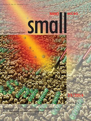
Small Vol. 10, Iss. 23, p. 4865 (2014)
Jian-Ying Huang, Yue-Kun Lai, Fei Pan, Lei Yang, Hui Wang, Ke-Qin Zhang, Harald Fuchs and Lifeng Chi
Multifunctional Superamphiphobic TiO2 Nanostructure Surfaces with Facile Wettability and Adhesion Engineering
A bottom-up, ink-combination method to rapidly achieve a water wettability and adhesion transition in situ with a great contrast on super-amphiphobic TiO2 nanostructured films is developed. On page 4865, Y.-K. Lai, K.-Q. Zhang, L.-F. Chi, and co-workers show why the multifunctional superamphiphobic TiO2 nanostructure surfaces with switchable wettability and adhesion engineering are excellent templates for microdroplet manipulation (storage, moving, mixing, and transfer), positive and negative micropatterning, specific gas sensing, and site-selective biomedical scaffolds.
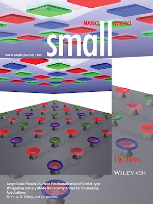
Small Vol. 10, Iss. 19, p. 3863 (2014)
Uwe Bog, Falko Brinkmann, Heinz Kalt, Christian Koos, Timo Mappes, Michael Hirtz, Harald Fuchs and Sebastian Köber
Large-Scale Parallel Surface Functionalization of Goblet-type Whispering Gallery Mode Microcavity Arrays for Biosensing Applications
To enable competitive biomolecular screening of complex analytes, dense and selective surface functionalization of sensor transducers is imperative. On page 3863, M. Hirtz, S. Koeber, and co-workers report a novel technique allowing the large-scale deposition of functional inks onto individual chip-based sensors. Polymer pen lithography-prepared glass slides act as custom stamp pads to directly print biochemical acceptor molecules. The technique is applied to densely packaged arrays of whispering gallery mode microgoblet cavities, which are then shown to function as biosensors.
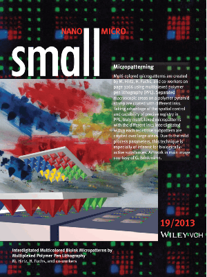
Small Vol. 9, Iss. 19, p. 3266 (2013)
Falko Brinkmann, Michael Hirtz, Alexandra M. Greiner, Markus Weschenfelder, Björn Waterkotte, Martin Bastmeyer and Harald Fuchs
Interdigitated Multicolored Bioink Micropatterns by Multiplexed Polymer Pen Lithography
Multi-colored micropatterns are created by M. Hirtz, H. Fuchs, and co-workers on page 3266 using multiplexed polymer pen lithography (PPL). Separated macroscopic areas on a polymer pyramid stamp are coated with different inks. Taking advantage of the spatial control and capability of precise registry in PPL, truly multiplexed micropatterns with the different inks interdigitated within each repetitive subpattern are created over large areas. Due to the mild process parameters, this technique is especially of interest for biologicallyactive substances. Artwork in main image courtesy of G. Brinkmann.
Small Vol. 8, Iss. 4, p. 487 (2012)
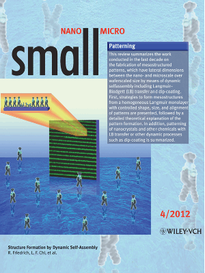
Liqiang Li, Michael Köpf, Svetlana Gurevich, Rudolf Friedrich and Lifeng Chi
Patterning: Structure Formation by Dynamic Self-Assembly
This review summarizes the work conducted in the last decade on the fabrication of mesostructured patterns, which have lateral dimensions between the nano- and microscale over waferscaled size by means of dynamic selfassembly including Langmuir–Blodgett (LB) transfer and dip-coating. First, strategies to form mesostructures from a homogeneous Langmuir monolayer with controlled shape, size, and alignment of patterns are presented, followed by a detailed theoretical explanation of the pattern formation. In addition, patterning of nanocrystals and other chemicals with LB transfer or other dynamic processes such as dip-coating is summarized.
Small Vol. 8, Iss. 4, p. 477 (2012)
Small Special Issue: Multilevel Molecular Assemblies, TRR 61
Inspired by natural systems and their fascinating properties, and facing the unsolved problems in molecular assemblies and their high scientific and economic potential, the DFG of Germany and the NSFC of China have jointly supported an interdisciplinary team of physicists, chemists, and biologists since 2008. The team comprises scientists from the University of Münster and the Tsinghua University in Beijing, as well as from Münster's Center of Nanotechnology and two institutes of the Chinese Academy of Science. Their objective is to develop multilevel molecular assemblies within the framework of a transregional collaboration, “Multilevel Molecular Assemblies: Structure, Dynamics, and Function,” which is also known as TRR 61. The selection of papers in this issue displays representative research activities of TRR 61, which is an excellent example of scientific collaboration between Germany and China. TRR 61 will hopefully inspire more international collaboration of this type because combining two different ways of thinking can result in startling advancement.
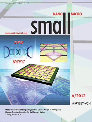
Small Vol. 8, Iss. 4, p. 557 (2012)
Yaling Liu, Meng He, Qing Meng, Zhiyong Tang, Liqiang Li and Wenping Hu
Mass-Production of Single-Crystalline Device Arrays of an Organic Charge-Transfer Complex for its Memory Nature
The cover image shows organic single-crystalline devices and device arrays, which are challenging to fabricate in situ. Single-crystalline lamellae of a charge-transfer complex, copper 7,7,8,8-tetracyano-p-quinodimethane (CuTCNQ), are synthesized in a controlled manner, and devices and device arrays of the lamellae based on symmetrical gold electrodes are efficiently mass-produced in situ. All the devices exhibit promising semiconductor properties, which are important for understanding the switching nature of the material. Moreover, the in situ fabrication of the single-crystalline devices and device arrays are attractive for the field of organic electronics, and they open up prospects for large-scale production of high-quality organic devices and circuits.
Small Vol. 3, Iss. 1, p. 71 (2007)
Steven Lenhert, Peng Sun, Yuhuang Wang, Harald Fuchs and Chad Mirkin
Massively Parallel Dip-Pen Nanolithography of Heterogeneous Supported Phospholipid Multilayer Patterns
The cover picture illustrates the use of self-organizing phospholipids as an ink for massively parallel dip-pen nanolithography. With this constructive lithographic technique it is possible to build model lipid-membrane patterns with sub-micrometer line widths over square-centimeter surface areas. The ability to pattern and integrate different membrane components opens many new possibilities in the fabrication of model systems that seek to simulate the chemical and structural complexity of biological membranes.

Springer ISBN 978-3-642-02404-7 (2010)
Bharat Bhushan and Harald Fuchs,(Eds.)
Biosystems- Investigated by Scanning Probe Microscopy
Essentials from the series “Applied Scanning Probe Methods” are put together in the area of bio and biorelated systems. The contributions spread over 13 volumes are now combined in this one volume. Thus, the reader will easily find a comprehensive overview of SPM applications for biosystems.
For scientists and professionals in academic and industry dealing with surface analytics of plant science, living cells, nanomedicine, cosmetics and biomimetics.

Springer ISBN 3-540-00527-7 (2004)
Bharat Bhushan, Harald Fuchs and Sumio Hosaka (Eds.)
Applied Scanning Probe Methods
V
V D I (2002)
Memorandum of Understanding zur wissenschaftlich-technologischen Zusammenarbeit Deutschland-Brasilien
Fact-Finding-Mission zur Nanotechnologie 4.-9. März 2002