
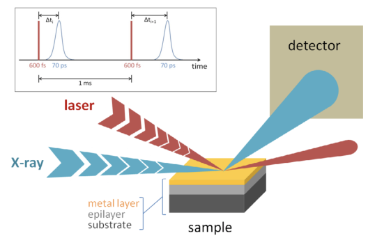
Thermal conductivity in silicon nanostructures
Nanostructuring enables new possibilities for the fabrication of materials with improved thermoelectric properties. The thermal conductivity of isotopically modulated silicon structures is analyzed with a time-resolved X-Ray scattering technique (TRXS) at the synchrotron in Grenoble (ESRF). By measuring the increased lattice constant of a gold layer, which covers the silicon nanostructure, and combining these results with numerical simulations, it is possible to obtain information about the thermal properties of the nanostructure. Sputter coating is utilized for the sample preparation and further studies involve atomic force microscopy and scanning electron microscopy. The samples are prepared in cooperation with the University of Aarhus and the Technical University of Braunschweig.
Contact person: Hartmut Bracht
Atomic transport in silicon and germanium
The diffusion of self-atoms and dopants in silicon and germanium single crystals is studied under various boundary conditions such as proton irradiation, extrinsic doping and in spatially confined nanostructures. For this purpose methods such as secondary ion mass spectroscopy (SIMS), spreading resistance profiling (SRP), atom probe tomography (APT) and scanning spreading resistance measurements (SSRM) are applied. Diffusion profiles are obtained and evaluated to gain new insight into the properties of dopants and the intrinsic point defects. This knowledge helps to develop suitable strategies for controlled diffusion doping of nanoscopic semiconductor structures.
Contact person: Felix Kipke
Optical properties in intercalation materials
Optical modulators are important components in integrated optical systems. The optical properties of these modulators can be manipulated by different physical processes. The injection of electrons and ions allows to change the optical behavior of electrochromic materials. Applying an electric potential will then change the material composition and by this its optical properties. This mechanism can be used to fabricate an electrically controllable optical modulator for photonic applications. One such material is vandium oxide (V2O5), a cathode material used in lithium-ion battery technology. The V2O5 layer structure can reversibly incorporate lithium ions by which its optical refractive index is affected.
Contact person: Felix Kipke
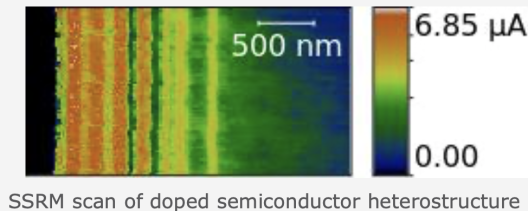
Scanning spreading resistance measurements on semiconductors
The analysis of electrically active dopant concentrations in nanostructred semiconductor components is a great challenge. Using scanning spreading resistance measurements (SSRM) with an atomic force microscope (AFM) offers an exciting opportunity to investigate the local spreading resistance and by this the electrical active dopant concentration in semiconductors with nanometer precision. Important parameters in such experiments are a sensitive sample preparation, a good electrical contact between the AFM tip and the sample as well as a reliable calibration of the measured resistance.
Contact person: Tim Böckendorf
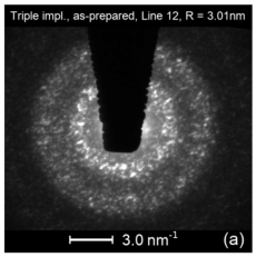
Structural analysis of amorphous semiconductors
Ion-implanted amorphous silicon is analyzed in terms of its disordered structure. For this purpose fluctuation electron microscopy (FEM) measurements are performed with an FEI Titan Themis G3 300 transmission electron microscope. FEM allows to study amorphous materials in terms of their medium range order (MRO). In this technique a series of diffraction patterns on different sample positions is collected using differently sized electron beams. Next, the diffraction patterns are evaluated to yield the variance. This quantity is sensitive to MRO and enables to partly interpret amorphous structures.
Further experiments are focussed on electron correlation microscopy (ECM). In ECM the nanoscale strucutral dynamics of amorphous materials are studied at elevated temperatures. The aim of these studies is to compare self-diffusion in amorphous silicon on the nanoscale to macroscopic measurements.
Contact person: Hartmut Bracht
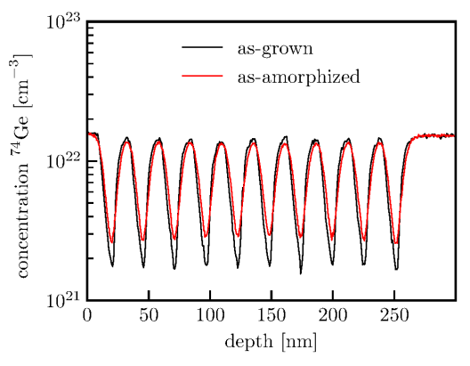
Structure and transport properties of amorphous silicon and germanium
The self-diffusion in isotopically modulated, amorphous silicon and germanium layer systems is studied by secondary ion mass spectroscopy (SIMS). The samples are fabricated by molecular beam epitaxy (MBE) on silion-on-insulator and germanium-on-insulator wafers and afterwards completely amorphized by ion implantation. Annealing these samples at different temperatures and times leads to a thermal broadening of the isotope structures, whose analysis yields the self-diffusion coefficient. These experiments combined with large-scale molecular dynamics simulations performed on GPUs provide information about the atomic structure and dynamics of amorphous silicon and germanium.
Contact person: Tim Böckendorf