Synthesis

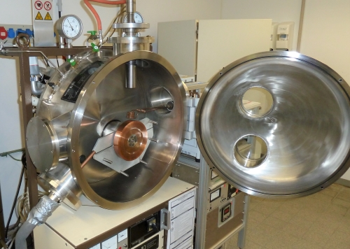
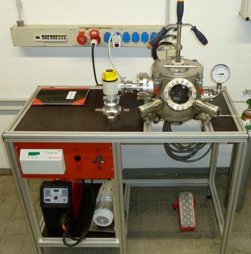
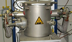
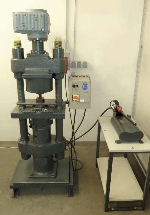
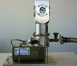
For the synthesis of different kinds of materials the members of the institute have access to well equipped chemistry labs and different kinds of technical equipment for cutting, grinding and polishing as well as equipment for direct synthesis like sputtering or coating machines. The mechanical workshop of the institute designs new facilities or modifies existing equipment in close collaboration with the scientific staff. Further more there are special devices in the institute like an arc-melter to prepare metallic alloys, special furnaces for sample treatments or a melt-spinner for metallic glass preparation etc. The most important devices for materials synthesis, which are accessible in the institute, are summarized in the list below:

  • Thermal synthesis and processing

    Meltspinner HV
    © IMP

    Meltspinner HV (Edmund Bühler)

    • tangential wheel speed up to 50 m/s
    • melting temperature up to 1500 °C
    • convertible to copper-mold casting


    arc melter
    © IMP

    Arc melter

    • pre-alloying of high melting metals
    • Vacuum up to 10-6 mbar
    • Currents up to 300 A
    • Temperatures above 2000 °C can be reached
    • Synthesis of metallic samples of up to 15 g
    • Meltung under inert gas atmosphere in water cooled copper casting molds


    Annealing furnace and RoF

    6 x annealing furnace SR 70-750/11 (Gero)
    1 x RoF 7/75 and 3 x RoF 4/50 (Heraeus)

    • anealing in air and argon
    • maximum temperature 1100 °C (Gero) and 1300 °C (Heraeus)


    Vacuum furnaces

    2 x vacuum furnaces SR 70-500/11 (Gero)

    • annealing in vacuum down to 1x10E-8 mbar
    • maximum temperature 1100 °C


    Oil oven

    Oil oven Phoenix II (Thermo Scientific)

    • annealing up to 180 °C
    • very low thermal fluctuations of 0,1 °C


    High temperature furnace

    High temperature furnace

    • High-temperature diffusion experiments in SiC
    • Tmax: ~ 2500°C


    Multi-zone furnace

    Multi-zone furnace

    • Resistance furnace with up to ten separate heating zones
    • Tmax: 1300°C


  • coating methods

    PVD-system

    PVD-system Auto 306 (Edwards)

    • evaporation with two thermal sources
    • evaporation with one e-beam source equipped with a 4 pocked rotary holder
      (simultaneously usable with thermal sources)
    • high vacuum up to 10E-7 mbar
    • modified for low temperature sublimation of organic molecules incl. a heated sample holder


    CVD-system

    CVD-system (self-made)

    • 3-zone-furnace to obtain a temperature gradient
    • maximum temperature 1100 °C
    • 3 separate gas inlets, one equipped with a digital flow meter
    • digital pressure control
    • working pressure down to 10E-3 mbar


    Savannah 100 ALD-system

    Savannah 100 ALD-system
    (Cambridge NanoTech)

    • monolayer accurate deposition of oxide on surfaces with high aspect ratios
    • up to four precursor installed at the same time


    potentiostats / galvanostats

    Potentiostats / galvanostats

    PGSTAT 302N (Autolab)
    • 2, 3 oder 4 electrode-setup
    • maximum potential +- 10 V
    • potentiostat bandwith 1 MHz
    MOD 7050 (Amel Instruments)
    • 2,3 oder 4 Electrode-setup
    • maximum potential +- 45 V
    • maximum current 4 A


  • TEM preparation

    PIPS

    Model 691 PIPS (Gatan)

    • Precision Ion Polishing System for TEM preparation
    • thinning with argon ions by two guns with variable incident angles
    • backlight, sight glass und optical microscope for process control


    Dimple Grinder

    Model 650 Dimple Grinder (Gatan)

    • for mechanical thinning of TEM samples down to several µm
    • double rotation system for homogeneous thinning


    © IMP

    TenuPol-5

    • Twin-Jet Elektropolisher Tenupol-5 (Struers) for thinning electron transparent foils (< 100 nm)
    • tunable voltages: 0 - 40 V
    • cooling device for different electrolytes


  • Mechanical processing

    HPT-press
    © IMP


    HPT-press (self-made)

    • up to 4 GPa static pressure
    • variable rotation speed


Analysis

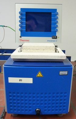
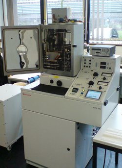
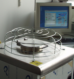
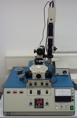
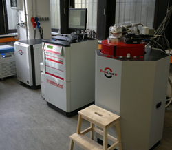
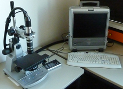
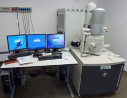
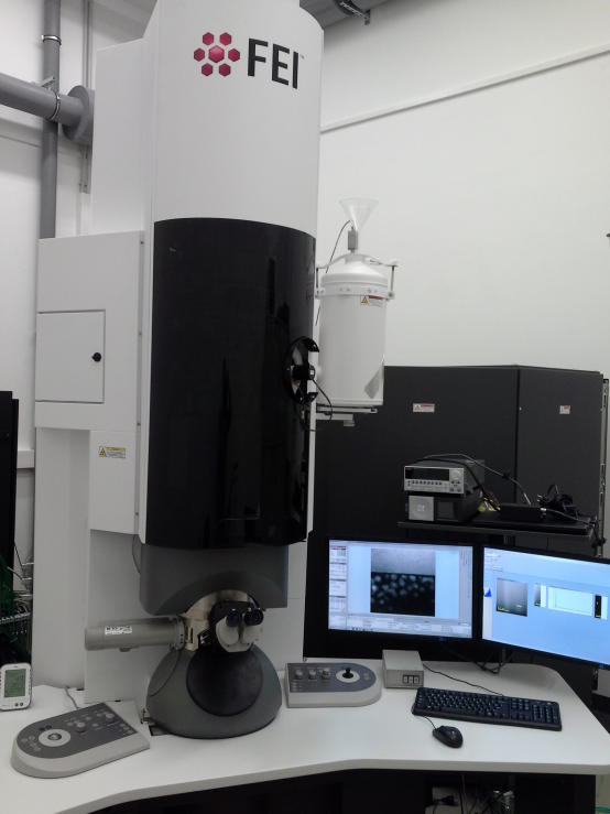
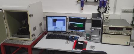
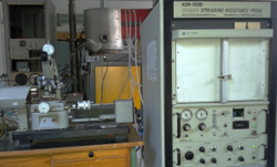
Of course the Institute of Materials Physics provides a broad range of facilities for materials analysis within the interdisciplinary research area covered by the groups that work in our institute. These facilities range from chemical analysis or calorimetry to structure analysis on the atomic scale, to mention just a few examples. A special position takes our isotope lab, where radiotracer measurements are used to determine diffusion behavior and diffusion mechanisms. Classical microscopy is also an important part of an institute in the field of materials physics. Thus, we employ several optical microscopes, but also scanning electron-, transmission electron- and atomic force microscopes, respectively with special equipment for sample preparation. Additionally, we have strong foci on tomographic atom probe tomography, on the electrical characterization of semiconductors or polymer electrolytes, on calorimetry and thermal analysis and also on the mechanical characterization of materials with respect of their yield strength or hardness. The following list summarizes the most important devices that are used for analysis purposes:
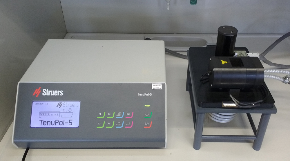
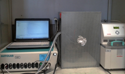
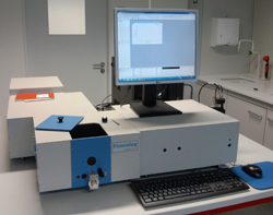
  • thermal analysis

    Diamond DSC

    Diamond DSC (Perkin Elmer)

    • liquid nitrogen thermostat
    • power compensated DSC for measurements from -170 °C to 500 °C
    • heating rates up to 500 K/min


    Labsys TG-DSC

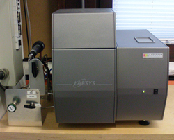
    Labsys TG-DSC (Setaram)

    • combined thermogravimetry und heat-flux DSC-measurements up to 1600 °C
    • modified for measurements in high purity argon atmosphere


    Q100 DSC

    Q 100 DSC (TA Instruments)

    • heat-flux DSC for measurements from -80 °C to 500 °C
    • modulated DSC


    TAM III nano-calorimeter

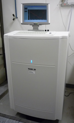
    TAM III nano-calorimeter (Thermometric)

    • high precision isothermal calorimetry up to 150 °C with a resolution of 10 nW
    • controllable gas flux


    Fast chip-calorimeter
    © IMP

    Fast chip-calorimeter (self-made)

    • Based on commercial sensor chips with a measuring area of 100 µm x 100 µm
    • Sample masses in the range of nanograms
    • Temperature range: 30 °C - 450 °C
    • Heating rates: 100 K/s - 10000 K/s
    • Integration in PPMS to measure in vacuum


    Drop-calorimeter

    HTC 1800K
    Drop-calorimeter (Setaram)

    • high temperature isothermal measurements
    • precision Cp-determination


    Dilatometer


    Dilatometer (Linseis)

    • precise determination of length changes by thermal expansion or phase transformation down to 0,1 µm
    • temperature range from -190 °C to 550 °C


    PPMS

    Physical Property Measurement System (PPMS)
    Evercool II (Quantum Design)

    • measurements from 1.9 K up to 400 K in a He-atmosphere or vacuum/high-vacuum.
    • Resistivity option: DC resistivity measurements
    • ACT option: AC resistivity measurements, Hall-effect, I-V-curves, critical current
    • HC option: measurements of the specific heat capacity
    • TTO option: thermal transport properties as heat conductivity, Seebeck-coefficient, el. conductivity, Figure of Merit, Nernst effect
    • ACMS option: measurement of the AC-susceptibility
    • VSM option: vibrating sample magnetometer to measure the DC-magnetisation and hysteresis curves (9-tesla magnet)


  • Microscopy

    VHX 500K digital microscope

    VHX 500K digital microscope (Keyence)

    • modular digital microscope with 200x magnification and 2 MPixel
    • 3D depth measurements with analysis function
    • software for automatic picture analysis concerning particle size and number


    Nova Nano SEM

    Nova Nano SEM 230 (FEI)

    • high resolution imaging with up to 30 kV
    • low-vacuum-modus for non-conductive or contaminating samples
    • Pt-injection system
    • EDX-detector (EDAX) for localized element analysis
    • EBSD-detektor for localized determination of crystal orientations (utilizable with EDX)


    Titan Themis G3 300 TEM
    © IMP

    Titan Themis G3 300 TEM (FEI)

    • Sub-Angström resolution of 80 pm
    • Ultrafast quadrupole EDX detector
    • Monochromator with energy resolution of < 200 meV
    • Detection of electromagnetic fields using a segmented detector for differential phase contrast (DPC)
    • Lorentz lens for magnetic imaging
    • Ultrafast EELS (1000 spectra per s)
    • Ultrafast in-situ CMOS camera (4k x 4k)
    • Z contrast imaging using HAADF detector
    • TEM holders for straining, heating, cooling, inert gas transfer
    • Software for strain analysis, focus series reconstruction, etc.


    Atomic Force Microscope Systems
    © IMP
    Atomic Force Microscope Systems
    © IMP

    Atomic Force Microscope Systems XE-100 (PARK)

    • separate X-Y and Z scanner
    • High- and low voltage mode for improved resolution
    • modular setup for future use of EFM, MFM, ...


  • X-ray analysis

    X-ray diffractometer

    D5000 X-ray diffractometer (Siemens)

    • Cu or Cr anode
    • size and strain analysis of poly-crystalline and powder samples
    • in- und ex-situ analysis of crystallizing amorphous material
    • one device is equipped with a heating chamber for in-situ experiments up to 600°C in vacuum or protective atmospheres


  • mechanical analysis

    material testing machine

    material testing machine 1195 (Instron)

    • maximum load 50 kN
    • additional external displacement sensor
    • free programmable computer controller
    • load cycle is possibleadditional oven for deformation under elevated temperatures


    Miniature material testing machine

    Miniature material testing machine (self-made)

    • Creep and uniaxial tensile testing via LabVIEW control
    • Forces
      • Maximum: 200 N
      • Accuracy: ±0,4 μm
    • Displacement
      • Maximum: 2000 μm
      • Accuracy: ±1,5 μm
    • Maximum temperature: 200 °C
    • Sample dimensions (dog-bone shape)
      • Gauge width: 150 μm - 550 μm
      • Gauge thickness: 40 µm - 2000 µm
      • Gauge length: 4000 µm


    nano-indenter
    © IMP

    Nano-Indenter (FemToTools FT-NMT04-XYZ)

    • Berkovich and Cube-corner tips
    • Force range: 0.5 nN to 200 mN
    • Noise floor: 500 pN and 50 pm
    • continuous stiffness measurements
    • 96 kHz for force and displacement control


    micro-indenter


  • electrical analysis

    4200-SCS


    4200-SCS (Keithley)

    • setup for precision electrical characterization of conductors and semi-conductors
    • conductivity, capacity, transistor characteristics...
    • heating stage


     Low-temperature cell with Closed Cycle Kryostat


    Low-temperature cell with Closed Cycle Kryostat

    • Electrical measurements at temperatures between 20 K and room temperature


    Spreading resistance Profiler


    Spreading resistance Profiler ASR 100B (SOLID STATE MEASUREMENT INC.)

    • Depth-resolved two point resistance measurement for determination of dopant profiles in semiconductors


    Potentiostat / Galvanostat Autolab

    Potentiostat / Galvanostat Autolab PGSTAT128N (METROHM)

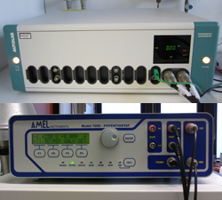
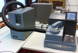
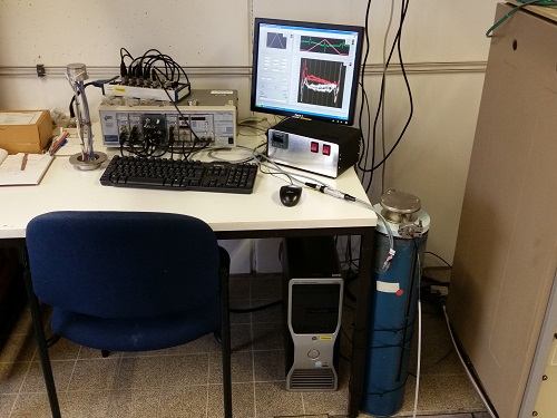
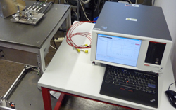
    • Setup for impedance spectroscopy measurements and temperature / pH measurements
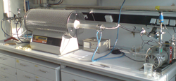
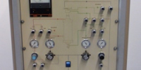
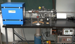


  • other

    Spectrometer Fluorolog

    Spectrometer Fluorolog III (HORIBA)

    • high power gas discharge lamp
    • double monochromator in excitation and emission
    • adjustable specimen holder for solids and liquids
    • FrontFace and RightAngle-option


    Flow-through furnace with mass spectrometer


    Flow-through furnace with mass spectrometer

    • Annealing under varying gas atmospheres
    • Gas analysis by mass spectrometer


All pictures: © Institute of Materials Physics