
Functional surface nanostructures
Nanostructured inorganic/organic hybrid materials offer an increased and new potential for diverse applications in a broad range of fields, such as gas-sensing or bio-sensing, optically active or optically responsive surfaces, with regard to novel solar cells of organic light-harvesting complexes or the wide range of organic electronics. Common to all such hybrid systems are complex electronic interactions at the interfaces between an inorganic substrate, which is structured in many cases, and complex functional molecules or organic/biological building blocks. Moreover, non-linear feedback through this complex interface is of particular significance regarding the functionality and stability of the hybrid nanostructures.
In general, such mechanisms need to be considered for the transport of information (photons, charges, masses) through complex interfaces. However, these mechanisms, which are crucial for the functionality and efficiency as well as the stability and lifetime of complex hybrid systems, are not completely understood so far. To experimentally investigate such complex interactions, it is necessary to prepare precisely controlled hybrid systems, which can be analyzed regarding the atomic and electronic structure of the interfaces, applying methods with high resolution. These results are then being incorporated in a model description of ensemble properties, which can be directly compared to results obtained from macroscopically averaging experimental analyses.
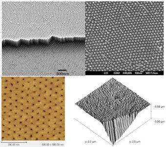
Synthesis of 3-dimensional nano-architectures
We synthesize semiconducting substrates, isotope-hetero structures, nanostructured semi-conducting, isolating and metallic surfaces as well as nanoporous templates of a precisely controlled, highly regular topology and microstructure. These structures are then functionalized by physical or chemical methods and the resulting hybrid systems are analyzed with regard to the atomic structure of the interface. Here, the expertise of materials physics is of particular importance, not only to quantitatively explore the topology but also to analyze the complex structure of defects at and within the interfaces and their impact on the functional properties of the hybrid composite.
Analyses of structures and properties with high spatial resolution
Essential for these studies is the possibility to perform high-resolution transmission electron microscopy without the delocalization of structural information by spherical aberration on “edge-on” oriented interfaces. At the same time, information on the local distribution of chemical elements, their oxidation states, on atomic level stresses and strains and on the presence, magnitude and direction of local electric or magnetic fields are required for a complete understanding. Those parameters are measured with atomic resolution by advanced analytical high resolution TEM using our Titan Themis G3 300 making (sub-) atomic resolution materials analysis and characterization available. The device allows direct imaging of the atomic structure, electron energy loss spectroscopy with high spectral resolution using a monochromator, and elemental mapping of monolayers thanks to a four-quadrant energy-dispersive X-ray spectrometer. A fast CMOS camera together with a comprehensive set of special specimen holders enables tracing reactions or transformations as a function of temperature, sample environment, mechanical or electrical attenuation. This exhaustive configuration serves to attain a much more detailed and sound comprehension of elementary processes at the atomic scale that determine macroscopic materials properties.
For more information, please visit the Wilde research group website.