Principal set-up of the IR converter
The basic design of the cell module and its operation is illustrated in following figure.
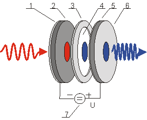
Exploded view
of the cell module. (1) electrical contact which transparent in
the IR; (2) semiconductor; (3) spacer; (4) gas discharge gap; (5) electrical
contact which transparent for visible light; (6) plate-glass; (7) dc
voltage supply
The semiconductor (2) has an electrical contact (1) on the input which is transparent for the incoming IR radiation. The diameter of semiconductor is in the order of 30 mm. The gas discharge layer (4) is in direct contact with semiconductor wafer, and its dimensions are limited by the dielectric spacer (3) which has a thickness in the range from 10 to 100 µm and an inner diameter of typically 25 mm. This diameter restricts the active area of the IR converter. Pure He, Ne, Ar, N2 or mixtures of these gases can be used as filling gas. The electrical contact (5) on the output is transparent for wavelengths in the visible range and is deposited on the glass substrate (6). The cell module is driven by a source of dc voltage which value is typically in the range of 600 to 1000 V. As to a basic principle, the IR converter operates as follows. Incoming IR radiation field increases locally conductance of semiconductor due to intrinsic photoeffect. This results in local increase of current density in the discharge space, which is accompanied by the local increase of emission of photons in the visible. In good approximation, the brightness of the outgoing light density emitted by the gas discharge is proportional to incoming IR radiation density. Converted images are recorded with a suitable camera which is sensitive in the visible.