Semiconductor-organic interfaces: Structural and electronic properties
Semiconductor-organic hybrid structures have gained increasing interest since they provide a large variety of applications, e.g. in the context of bio-sensing or light emitting devices. While a suitable organic adsorbate has to be chosen for the specific purpose, the inorganic substrate has to be compatible to our present-day electronics. The electronic and optical properties of semiconductors are well-known and tunable by doping and band gap engineering. Therefore the use of semiconducting substrates is advantageous in contrast to metal substrates. Hence much effort is made to understand the structural and electronic properties of semiconductor-organic interfaces.
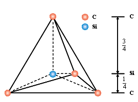 Silicon carbide (SiC) represents a group IV two-compound semiconductor with a large bandgap up to 3.3 eV. The Si and C atoms exist in the stoichiometric ratio of 1:1 in the bulk, but not necessarily at the surface. Thereby each Si-atom is surrounded by 4 C atoms forming a tetrahedron. The Si-atom is not located in the centre of the tetrahedron, but it is moved about one fourth above the basis plane (see left figure). Thus the Si and C atoms form alternating bilayers. One specialty of SiC is the formation of different crystal structures (polytypes) depending on the stacking sequence of the tetrahedrons. More than 170 different polytypes of SiC are known today. The most well-known and most investigated ones are the hexagonal polytypes 6H-SiC and 4H-SiC and the cubic 3C-SiC.
Due to its outstanding properties, like a high saturation electron drift velocity, a high breakdown field and excellent thermal conductivity it is a promising material for high temperature and high power applications (see following table). On the other hand SiC is well suited for semiconductor-organic hybrid structures due to its biocompability and non-toxicity. Therefore it is a suitable substrate for the creation of organic-inorganic hybrid structures.
| Si | GaAs | 3C-SiC | 6H-SiC | diamond | |
| bandgap at 300 K (eV) | 1,12 | 1,43 | 2,3 | 2,9 | 5,5 |
| thermal conductivity (W/cmK) | 1,5 | 0,5 | 4,9 | 4,9 | 20 |
| max. operating temperatur (°C) | 150 | 460 | 600 | 1000 | 1100 |
| saturated electron drift velocity (km/s) | 100 | 100 | 250 | 200 | |
| break through field strength (kV/cm) | 250 | 300 | 2000 | 2500 | 10000 |
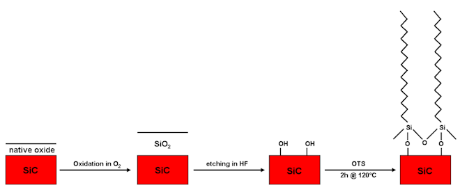
The intention of our work is the preparation of semiconductor-organic hybrid structures on SiC substrates and the investigation of its overall structural and electronic properties. The electronic properties are to a certain extend determined by the molecular levels of the adsorbed molecules as well as by the band structure of the underlying substrate. However, there may also appear a significant interaction between the substrate and adsorbate. One possible preparation route is the formation of self-assembled monolayers (SAMs) via wet chemistry or vapour deposition (see figure below). This preparation is carried out within cooperations with the groups of Prof. Dr. L. Chi and Prof. Dr. L. De Cola, respectively.
X-ray photoelectron spectroscopy (XPS) is used to analyze the elemental composition of the created interfaces. This non-destructive method is also a powerful tool to quantify the overlayer thickness and to investigate the bonding configuration of each element. Supplementary information of the occupied electronic states is provided by ultraviolet photoelectron spectroscopy (UPS).
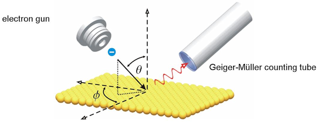
Inverse photoemission spectroscopy (IPE) allows the determination of the unoccupied electronic states of functionalized SiC surfaces. For this surface-sensitive technique, low energy electrons with energies between 2.0 and 30.0 eV are directed towards the sample under different angles of incidence (see figure below). The electrons reaching the surface emit photons with energies according to the difference of the kinetic energy of the incoming electron and the energy of the unoccupied electronic states above the Fermi level. The photons are detected with a Geiger-Müller counting tube. It is equipped with an entrance window of CaF2 and it filled with acetone. The transmission of the window together with the ionization threshold of the acetone acts as a bandpass of 400 meV width at a center energy of 9.9 eV. Plotting the intensity of these photons against the energy of the incoming electrons for a fixed angle in IPE-spectra provides information about the unoccupied states of SiC substrates and the energetic position of unoccupied molecular levels in the organic film. Furthermore a variation of the angle of incidence leads to angle resolved measurements and thus the momentum dependence of the bands.
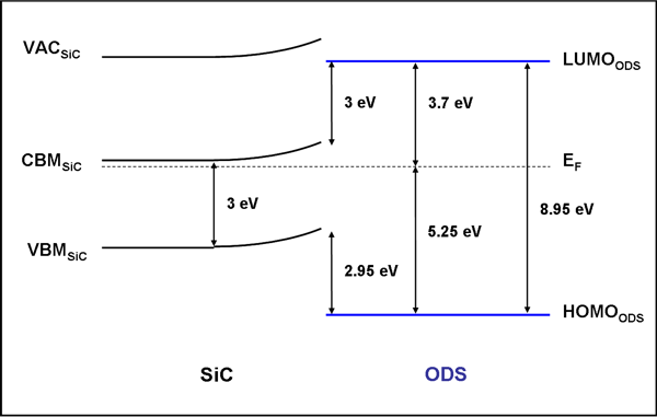
Because of the surface sensitivity of the techniques, all experiments are performed under ultra high vacuum (UHV) conditions. In this UHV chamber a pressure of less than 1x10⁻¹⁰ mbar is achieved. The chamber is equipped with a load-lock which allows a quick and comfortable sample exchange. A set-up for low energy electron diffraction (LEED) and a spectrometer for auger electron spectroscopy (AES) are also available in the UHV chamber. However, XPS and UPS are performed in a different UHV chamber in our group. The combination of all techniques provides a comprehensive view of the electronic structure of functionalized SiC surfaces e.g. a SiC-ODS interface (see figure below).