Wegner Group: Nanoscale Magnetism & Electronics

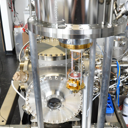
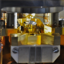
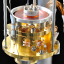
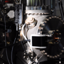
In order to study single molecules with atomic-scale resolution, we use a commercially available low-temperature STM system, the Createc LT-STM. It consists of a LHe cryostat surrounded by a LN2 cryostat (for thermal radiation shielding), all mounted into a ultrahigh vacuum (UHV) chamber in order to enable clean and controlled sample preparations. The STM is hanging underneath the LHe cryostat by spring suspension, surrounded by radiation shields to keep the sample temperature below 6K. Special shutters on the shields can be opened for low-temperature deposition of isolated metal atoms and molecules onto the sample.
The STM is not just a microscope: many additional experiments can be realized with the STM, making it a versatile tool that we like to refer to as an “integraded nano laboratory”. In the following sections we describe some of the various techniques that can be realized with an STM.
STM imaging
To get an STM image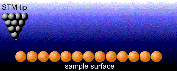 , a sharp metallic tip is scanned across a surface at a distance of less than one nanometer. The tunneling current between tip and sample (at a given applied voltage) is measured and an electronic feedback adjusts the tip-sample distance such that the tunneling current stays constant at all times. Thus the height of the tip versus its lateral position on the sample reproduces (in a simple picture) the corrugat
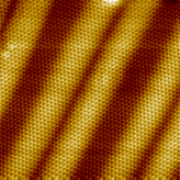 ion of the surface. Each specific height can be given a greyscale or color to create the STM image. The power of STM is its high spatial resolution. For almost any STM tip, there is always one atom sticking out a bit more than the others. As the tunneling current decreases exponentially with increasing tip-sample separation, almost all of the measured current goes through that outermost atom of the STM tip. Thus, as just one single atom probes the surface, it is rather easy to image surfaces with atomic resolution, for example the beautiful corrugated atomic structure of a gold surface as shown here. You can find more examples in our image gallery.
, a sharp metallic tip is scanned across a surface at a distance of less than one nanometer. The tunneling current between tip and sample (at a given applied voltage) is measured and an electronic feedback adjusts the tip-sample distance such that the tunneling current stays constant at all times. Thus the height of the tip versus its lateral position on the sample reproduces (in a simple picture) the corrugatSTM manipulation
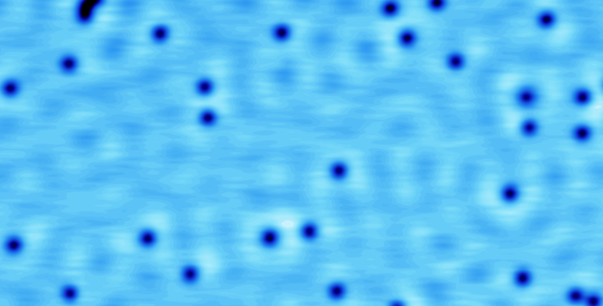
The STM tip can be used to move atoms and molecules on the surface in a controlled fashion. STM imaging is done with a rather large distance between tip and sample, typically 1 nm. But when the tip is brought very close to a single adsorbate (atom or molecule on top of a surface), there can be an attractive force between the two (like a temporary chemical bond). If this happens, the adsorbate will precisely follow the movement of the tip. So you can drag it wherever you want - with atomic-scale precision! This process can be repeated many times, e.g., in order to build a nanoscale structure with a certain function or to induce chemical reactions between different adsorbates in an ultimately controlled environment. In this example, we have moved more than 50 carbon monoxide (CO) molecules pecisely to well-defined positions on a copper surface (Cu(111)) to form the logo of the WWU Münster.
STS
STM-IETS
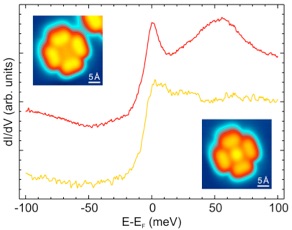
The tunneling electrons can also excite vibrations or spin-flips, which can be measured via inelastic electron tunneling spectroscopy (IETS). Usually, energy is conserved in the tunneling process. For example, when tunneling between the tip and a molecule that is adsorbed on a surface, elastic tunneling probes the LDOS of the molecu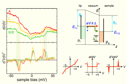 le, and we may be able to see peaks in dI/dV when the sample bias corresponds to the energy of the highest occupied (HOMO) or lowest unoccupied molecular orbital (LUMO).
However, the molecule also has vibrational degrees of freedom, and tunneling electrons are sometimes able to excite those vibrations. When doing that, the electrons lose the energy corresponding to the vibration and their final state is at a lower energy. Thus, we now have two channels for electrons to tunnel between tip and sample: the elastic channel with initial and final states at identical energies, and the inelastic channel where the final state is at lower energy. The additional channel „opens“ once the energy of the tunneling electrons is large enough to excite the vibration. This leads to a sudden increase of the slope in the I-V curve (the inelastic channel increases the conductivity), which corresponds to a step in dI/dV.
We have recently shown that combining the high spatial and energy resolution of STM-IETS opens the possibility to study more complex or inhomogeneous systems (e.g. where the vibrational mode is altered by the local adsorption geometry). We will extend the use of IETS in our lab toward detecting other correlated excitations (e.g. spin flips or magnon excitations in magnetic systems).
SP-STM
The STM tip can be “functionalized” by coating it with a magnetic thin film that makes it a spin-polarized STM (SP-STM). When scanning a magnetic sample, this makes a tunnel magnetoresistance (TMR) device where conductivity changes are caused by changing alignemt of tip and sample magnetization. Knowning the tip magnetization, one can thus image magnetic domains but also locally varying spin polarization of single atoms and molecules with unprecedented spatial resolution. Our Createc LT-STM allows in-situ heating and deposition of STM tips as well as tip exchange - necessary prerequisites to perform SP-STM experiements. We are currently equipping our UHV system with additional sample-treatment tools in order to soon perform SP-STM experiments on state-of-the-art complex magnetic samples.
AFM/STM
The STM tip is usually fixed to a rigid tip holder. But it can also be attached to a microscopic tuning fork that causes the tip to vibrate with high frequency (typically on the order of 10 kHz) but small amplitude (well below one nanometer). This setup allows for STM imaging (the tunneling feedback usually works at much lower bandwidths around 1 kHz), while simultaneously measuring the forces applied between tip and sample (e.g. a molecule on a surface). Our Createc LT-STM is already prepared for combined AFM/STM operation, and we are currently working on realizing our first AFM measurements.
Experimental Methods
Last Update: 25 Jan. 2016